STM32F4 Hardware Development
In this article, we will delve into the minimum system requirements for the STM32F4 MCU, covering aspects such as power, clocking, reset, startup modes, and debugging management.
Power Supply
The STM32F4 operates within a normal voltage range of 1.8-3.6 V (with certain exceptions mentioned in the datasheet, where it can go down to 1.7 V). Additionally, there is an integrated regulator that provides a 1.2 V digital power supply.
In cases of a main power loss (VDD), the RTC and backup registers can be powered by the voltage supplied to VBAT.
Pin Descriptions
ADC Power and Reference Voltage
To enhance conversion precision, the ADC has dedicated power pins that can be separately filtered to shield against noise on the PCB.
The ADC voltage source is connected to a separate VDDA pin. In circuit design, it's essential to connect VSSA to the same ground as VSS rather than VSS.
For packages with more than 100 pins, there are VREF+ and VREF- pins that provide external reference voltage to the ADC. VREF- should be connected to the internal VSSA. For packages with fewer than 100 pins, these pins are not exposed and are internally connected to VDDA and VSSA.
Backup Battery Supply
To retain the contents of the backup registers after a VDD power loss, VBAT can be connected to a battery or another power source. VBAT also supplies power to the RTC, controlled by the power-down reset (PDR) circuit within the reset module.
Built-in Regulator
The built-in regulator is always enabled after a reset and operates in three modes:
- Run: Provides full power supply (1.2 V domain) to the core, memory, and digital peripherals.
- Stop: Provides low power supply to the 1.2 V domain while retaining register and SRAM content.
- Standby: Regulator is powered down, and content in registers and SRAM, except for the standby circuit and backup domain, is lost.
Circuit Design
Here are the design considerations for power supply pins:
- VDD
- Decoupling Capacitors: A total of one 10 μF ceramic/tantalum capacitor, along with an additional 100 nF ceramic capacitor for each VDD pin.
- VDDA
- Decoupling Capacitors: 100 nF ceramic capacitor + 1 µF ceramic/tantalum capacitor.
- Filtering Analog Noise: Can be connected to VDD via ferrite beads.
- VREF+
- Decoupling Capacitors: If VREF+ function is enabled, connect a 100 nF and a 1 µF capacitor.
- Filtering Analog Noise: Can be connected to VDDA via a 47 Ω resistor.
- VBAT: Connect to an external battery (1.65 V-3.6 V). If a battery supply is not needed, connect to the VDD pin.
- VCAP1/VCAP2: Each should be connected to ground with a 2.2 µF ceramic capacitor (ESR < 2 Ω). If only VCAP1 is used, add a 4.7 µF ceramic capacitor (ESR < 1 Ω).
Reset and Power Monitoring
Power-On Reset (POR) / Power-Down Reset (PDR)
STM32F4 chips integrate POR/PDR circuits, and specific characteristics of power-on/power-down resets are depicted in the image above. To disable this feature, it can be achieved through the PDR_ON pin.
System Reset
System resets can be triggered by:
- NRST pin low level (external reset)
- Window watchdog timer count expiration (WWDG reset)
- Independent watchdog timer count expiration (IWDG reset)
- Software reset (SW reset)
- Low-power management reset
You can identify the reset source by examining the reset flags in the control/status register (RCC_CSR). Even if an external reset circuit is not required, adding a pull-down capacitor is recommended to enhance electromagnetic susceptibility (EMS) performance.
Clocking
On the STM32F4, there are three different clock sources to drive the system clock (SYSCLK):
- HSI (High-Speed Internal Clock)
- HSE (High-Speed External Clock)
- PLL Clock
There are also two secondary clock sources:
- LSI RC (32 kHz Low-Speed Internal RC) for driving the independent watchdog and automatic wakeup in RTC stop/standby modes.
- LSE (32.768 kHz Low-Speed External Crystal) for RTC operation.
If power consumption needs to be reduced, each clock source can be individually disabled when not in use.
External High-Speed Clock (HSE)
The HSE clock source can be provided in two ways: an external source (active) and an external crystal / ceramic resonator (passive).
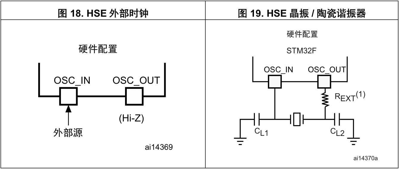
External Source (HSE Bypass)
If an active external clock signal is selected, a clock source of 1-50 MHz is required. Connect OSC_IN to an external clock signal with a duty cycle of approximately 50% (square wave, sine wave, or triangular wave), while keeping OSC_OUT in a high-impedance state.
External Crystal / Ceramic Resonator (HSE Crystal)
When an external crystal is chosen, the frequency range is 4-26 MHz. When designing the circuit, the resonator and load capacitors should be placed as close as possible to the oscillator pins to minimize output distortion and startup stability time. The value of the load capacitors should be adjusted accordingly based on the chosen oscillator.
Both CL1 and CL2 should use capacitors of the same size (5-25 pF, with a typical value of 25 pF).
External Low-Speed Clock (LSE)
The LSE clock source can be provided in two ways: an external source (active) and an external crystal / ceramic resonator (passive).
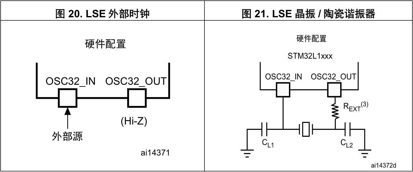
External Source (LSE Bypass)
If an active external clock signal is selected, a clock source below 1 MHz is required. Connect OSC32_IN to an external clock signal with a duty cycle of approximately 50% (square wave, sine wave, or triangular wave), while keeping OSC32_OUT in a high-impedance state.
External Crystal / Ceramic Resonator (LSE Crystal)
When an external crystal is chosen, the frequency range is 32.768 kHz, which can be used as the RTC clock source. When designing the circuit, the resonator and load capacitors should be placed as close as possible to the oscillator pins to minimize output distortion and startup stability time. The value of the load capacitors should be adjusted accordingly based on the chosen oscillator.
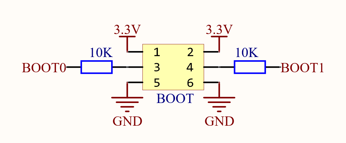
Boot Modes
Boot modes, also known as bootstrap modes, can be selected using the BOOT0 and BOOT1 pins to choose from three different startup modes: boot from the main flash memory, boot from the system memory, or boot from the internal SRAM.
For detailed information about boot modes, please refer to the article STM32 Boot Modes.
In most cases, a 10k ohm pull-down resistor is connected to BOOT0, and BOOT1 can be left unconnected. If mode switching is needed, you can refer to the following design:
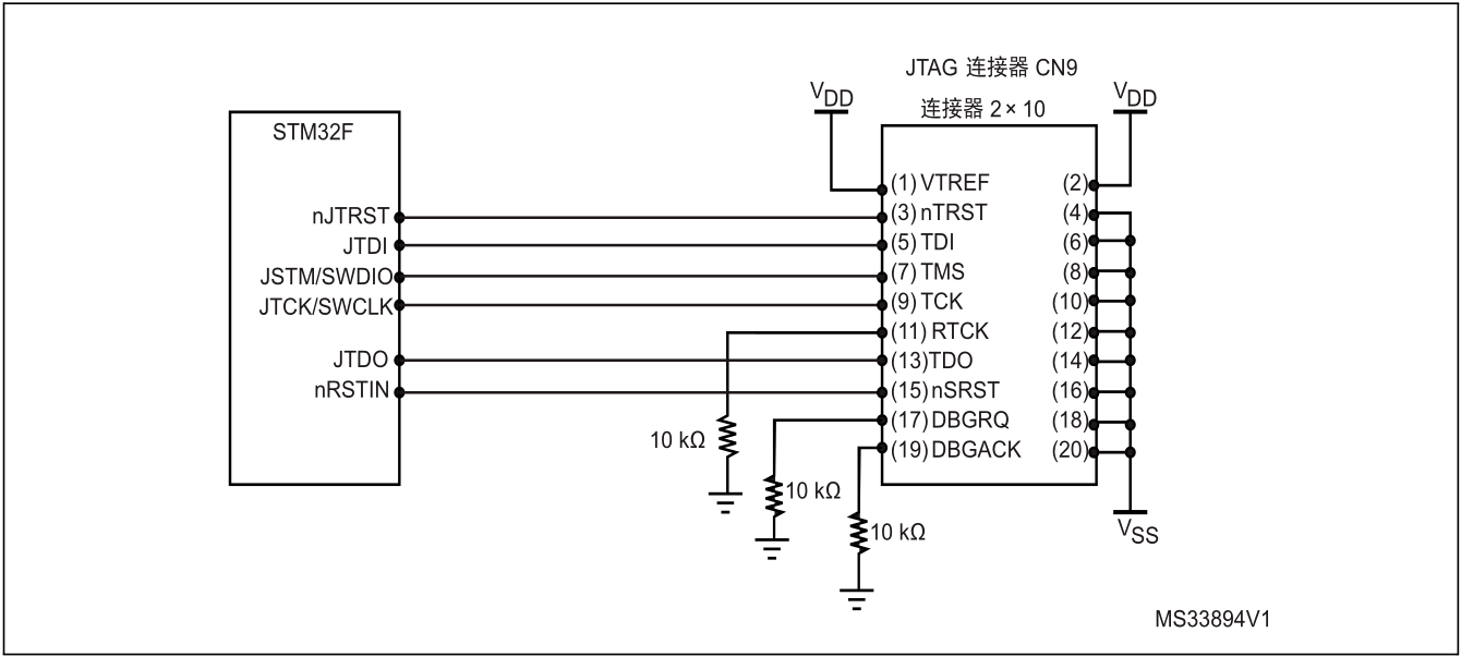
Debug Management
STM32 is typically used with the SWJ protocol for download and debugging.
SWJ Debug Port
The STM32F4 has a built-in SWJ (SW/JTAG) interface. SW-DP consists of 2 pins (clock + data), while JTAG-DP consists of 5 pins, some of which are multiplexed. For detailed differences, please see the article Differences and Connections between SWD and JTAG.
In STM32F4, the pin assignments for SWJ are as follows:
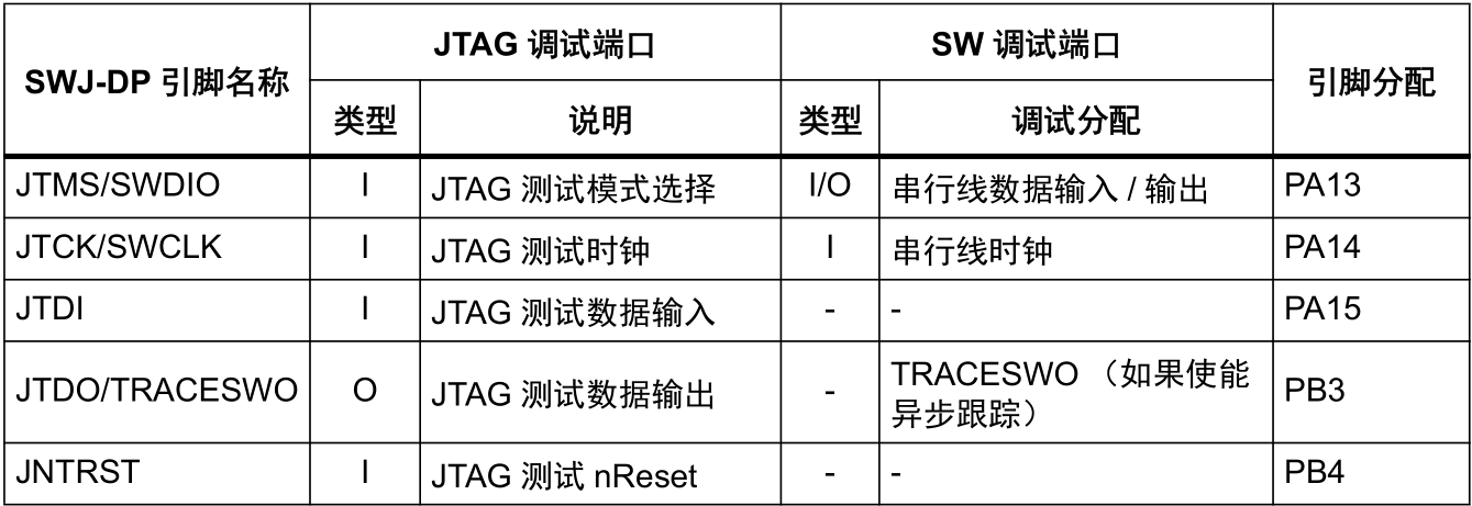
Internal Pull-Up and Pull-Down for JTAG
JTAG pins should not be left floating (as they are directly connected to trigger controls for debugging modes). Therefore, the chip internally integrates pull-up and pull-down for them:
- JNTRST: Internal pull-up
- JTDI: Internal pull-up
- JTMS/SWDIO: Internal pull-up
- TCK/SWCLK: Internal pull-down
Once software releases the JTAG I/O, they can be used as regular I/O ports.
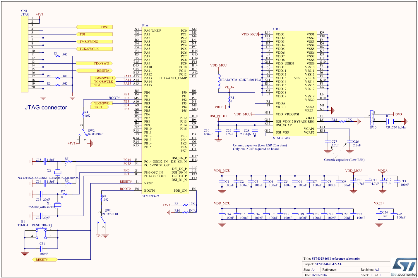
Hardware Design for Connecting a Standard JTAG Connector
Reference Design
References and Acknowledgments
Original: https://wiki-power.com/ This post is protected by CC BY-NC-SA 4.0 agreement, should be reproduced with attribution.
This post is translated using ChatGPT, please feedback if any omissions.