Designing the OSD335x Minimum System
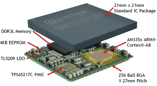
The OSD335x-SM chip from Texas Instruments integrates a Cortex-A8 AM335x processor, DDR3 memory, TPS65217C PMIC (Power Management Integrated Circuit), TL5209 LDO (Low Drop-Out Voltage Regulator), necessary passive components, and a 4KB EEPROM within a System-in-Package (SIP) module, all packaged in a BGA package.
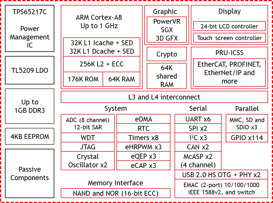
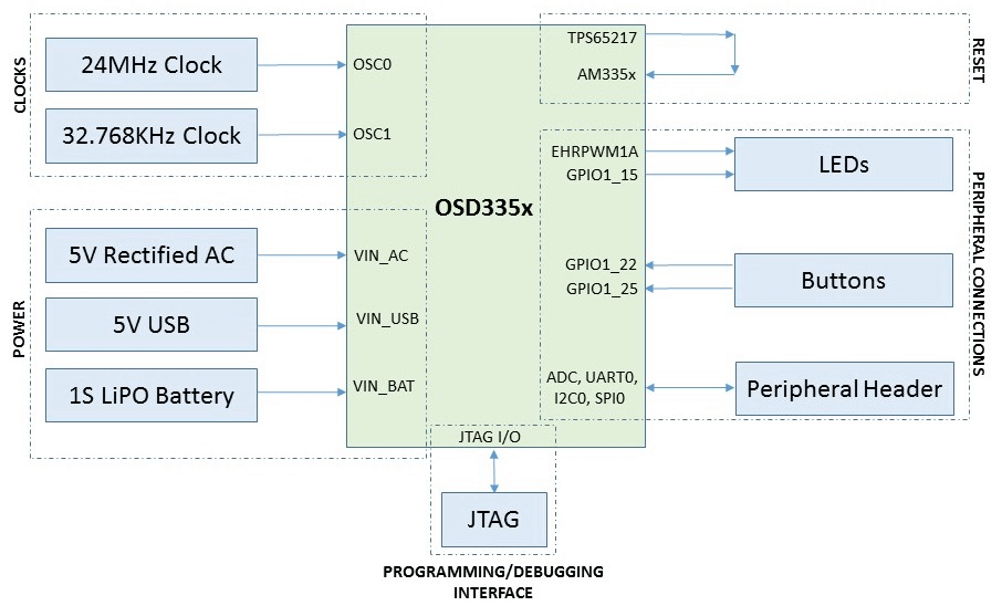
The minimum system for OSD335x consists of four main components: power supply, clock, reset, and programming/debug interfaces. To enhance usability, buttons, LEDs, and additional peripheral pins can be added.
Power Supply
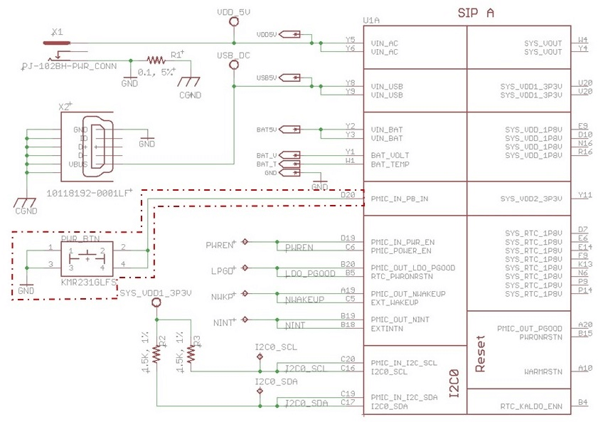
Input
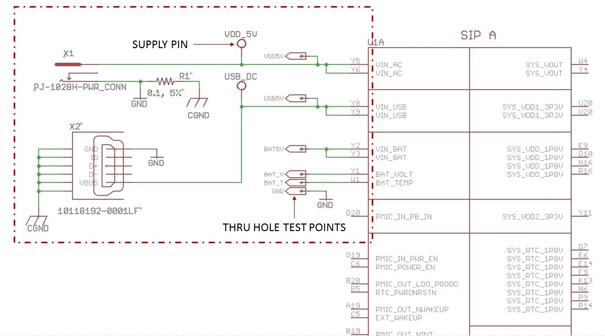
- VIN_AC: Main power input (DC 5V @ 2A), with the option to add a fuse, inductors, diodes, input protection, as needed.
- VIN_USB: USB power input (DC 5V @ 0.5A, can be increased to 1.3A through internal PMIC), also serves as the reference voltage and current for USB 2.0 host functionality.
- VIN_BAT: Can serve as a battery input (using battery power, 2.75-5.5V) or output (for battery charging), but cannot be used for events.
Output
- SYS_VOUT: Equal to the input voltage to the PMIC. Components connected to this pin should be compatible with the 3-5V range, as the PMIC switches between different power sources when charging the battery.
- SYS_VDD1_3P3V: 3.3V output, provided by TL5209 LDO and enabled by PMIC's LDO4, serving as the primary power output.
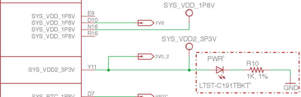
- SYS_VDD2_3P3V: 3.3V output, provided by PMIC's LDO2.
- SYS_RTC_1P8V: 1.8V output, provided by PMIC's LDO1 and used to drive the internal RTC of AM335x.
- SYS_VDD_1P8V: 1.8V output, provided by PMIC's LDO3.
- SYS_ADC_1P8V: 1.8V output, provided by PMIC's LDO3, includes filtering for analog applications and powers the AM335x ADC internally.
It is recommended to add test points to all power outputs for ease of debugging.
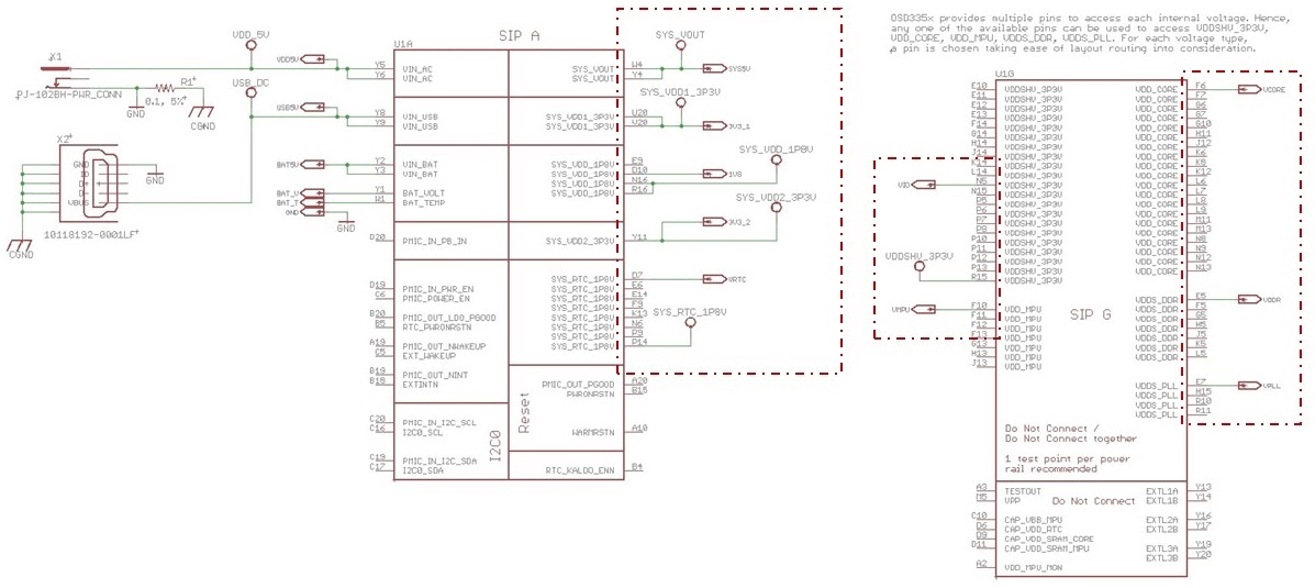
There are also some internal power supply pins: VDDSHV_3P3V, VDDS_DDR, VDD_MPU, VDD_CORE, VDDS_PLL. These are only meant for testing purposes and should not be connected to external circuits.
Analog Reference Inputs and Ground
OSD335x features an ADC interface, and for ADC to function correctly, it's essential to use the analog power supply and ground properly. The ADC interface can tolerate a maximum of 1.8V for analog input (referring to the VREFP pin). Typically, VREFP can be directly connected to SYS_ADC_1P8V, but if necessary, it can be divided to a lower voltage.
Power Management
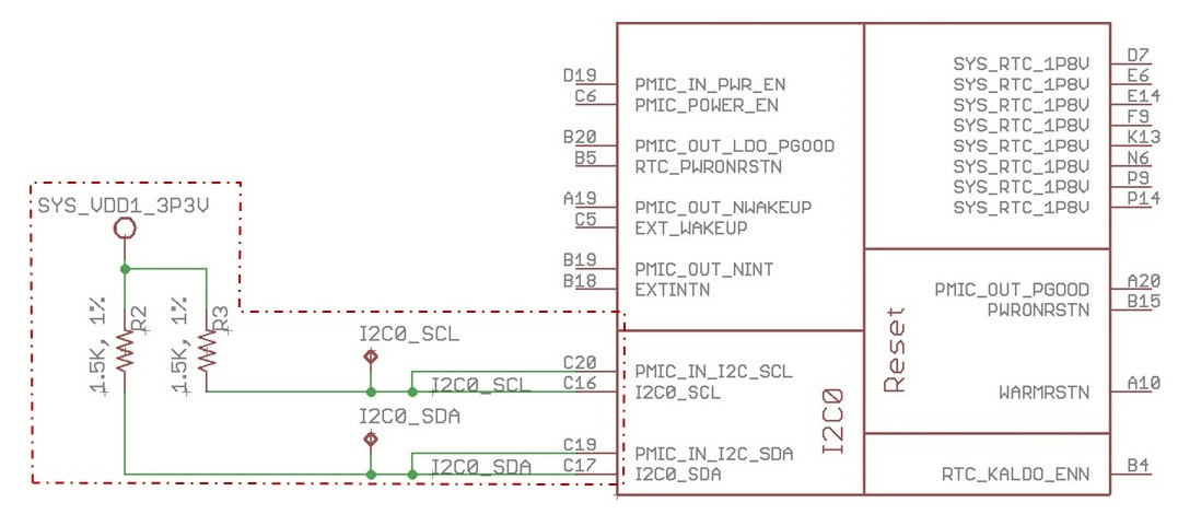
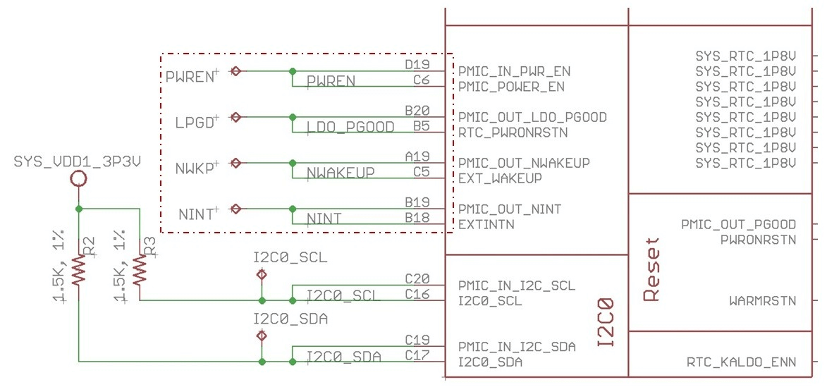
Internally, OSD335x communicates with the TPS65217C PMIC through I2C0. While I2C0 has internal 4.7k pull-up resistors, it's advisable to add external pull-up resistors when connecting devices.
The TPS65217C PMIC can be configured via I2C for the following parameters:
- Battery charging voltage
- Charging safety time control
- Buck/Boost output voltage
- LDO output voltage
- Power-on/power-off sequencing
- Overcurrent and over-temperature thresholds
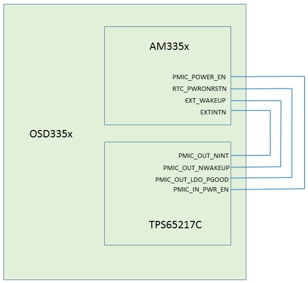
In addition to the I2C connection, the PMIC has some feature pins that need to be connected to OSD335x:
- PMIC_POWER_EN: This is used to control the power-up sequence of the PMIC for AM335x.
- PMIC_IN_PWR_EN: Enabling this signal for the PMIC's buck and LDO will initiate the power-up sequence control when a high-level signal is provided.
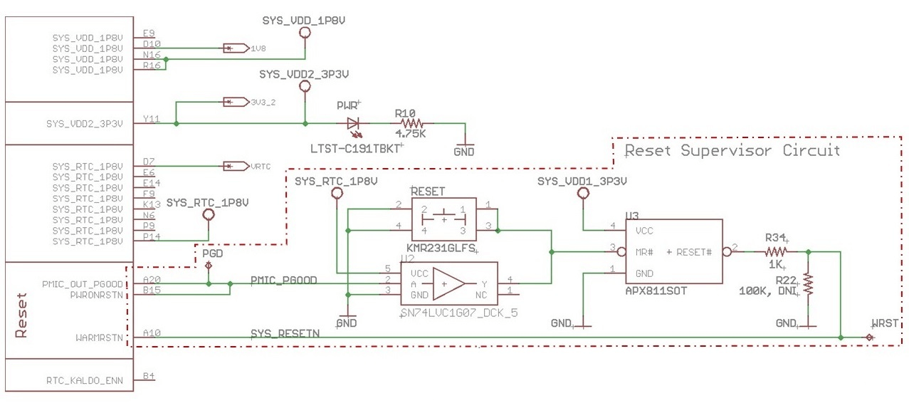
- RTC_PWRONRSTN: This is the independent power reset pin for the RTC on AM335x.
- PMIC_OUT_LDO_PGOOD: Indicates the output status of LDO1 and LDO2. A high-level signal indicates good output, while a low-level signal suggests an issue with either LDO.
- EXT_WAKEUP: This pin is used for external event wake-up.
- PMIC_OUT_NWAKEUP: Host external event wake-up pin (active low).
- EXTINTN: An external interrupt input pin for AM335x.
- PMIC_OUT_NINT: PMIC terminal output pin (active low).
Power Button
The TPS65217C PMIC features a low-level effective reset input, connected to the OSD335x through the PMIC_IN_PB_IN pin. It can also be connected to an external button. This input has a 50ms debounce time and an internal pull-up resistor. Additionally, the power button has the following functions:
- When PMIC_IN_PB_IN detects a falling edge input, it will wake the PMIC from a shutdown or sleep mode.
- If PMIC_IN_PB_IN remains low for more than 8 seconds, the PMIC will power up or reset.
- If the PMIC_IN_PB_IN pin remains low for an extended period, the device will cycle between the ACTIVE and RESET states, entering a reset every 8 seconds.
Power Indicator Light
We use SYS_VDD2_3P3V (150mA) as the output for the power indicator light.
Resets
OSD335x supports several reset modes:
- Cold Reset (Power-On Reset): Occurs during device power-up and power domain power-up.
- Warm Reset
- A partial reset that does not affect global logic.
- Designed to reduce reset recovery time.
OSD335x has three reset inputs (sharing names with AM335x's reset inputs):
- PWRONRSTN: Cold reset; must remain low during power-up until all input power rails stabilize; non-blocking and affects the entire system except for the RTC, which has its separate power-on reset.
- WARMRSTN: Warm reset; some PRCM (Power, Reset, and Clock Management) and control module registers are insensitive to warm reset.
- RTC_PWRONRSTN: RTC module-specific power-on reset input, not affected by cold reset, and does not impact other parts of the device.
Clocks
OSC0 and OSC1
OSD335x has two clock inputs:
- OSC0: High-speed clock input (main clock) operating at 19.2MHz, 24MHz (recommended), 25MHz, or 26MHz. This clock source serves as a reference for all non-RTC functions. OSC0 clock input includes OSC0_IN, OSC0_OUT, and OSC0_GND pins.
- OSC1: Low-speed clock input running at 32.768kHz for RTC. OSC1 clock input includes OSC1_IN, OSC1_OUT, and OSC1_GND pins. This clock source is disabled by default and is optional. If needed, it can receive an internal 32kHz RC crystal signal.
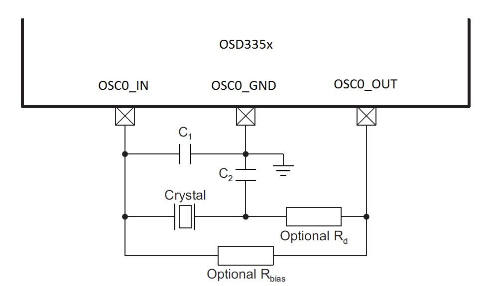
In the above diagram, Rbias and Rd are optional components. If precise frequency control is not needed, Rbias can be used for flexible calibration and can be designated as DNP (do not populate on the schematic or leave the position empty). However, if Rd is not needed, it must be replaced with a wire to avoid an open circuit.
In the reference design, OSC0 employs a 24MHz crystal oscillator, specifically the 7A-24.000MAAJ-T, with 18pF capacitors and a 1MΩ resistor serving as Rbias.
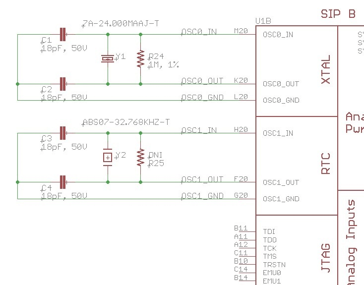
The RTC_KALDO_ENN pin is configured with an external pull-down using a 10k resistor to enable the internal RTC LDO.
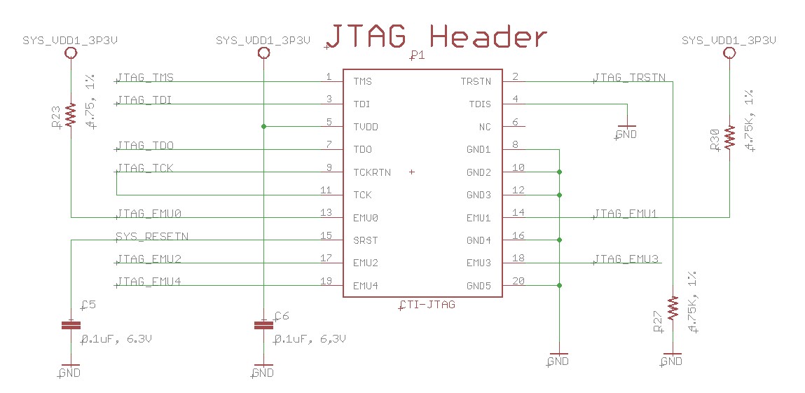
Flashing and Debugging Interface
In the reference design, a JTAG interface is used for flashing and debugging.
Other Peripherals
Boot Configuration
For boot configuration details, you can refer to the SYSBOOT Configuration Pins section in the AM335x Technical Reference Manual (TRM).
In the reference design, the following parameters are configured:
- Clock frequency set to 24MHz
- CLKOUT1 output disabled via XDMA_EVENT_INTR0; this pin is used solely for JTAG emulation.
- Boot sequence set to SPI0 -> MMC0 -> USB0 -> UART0
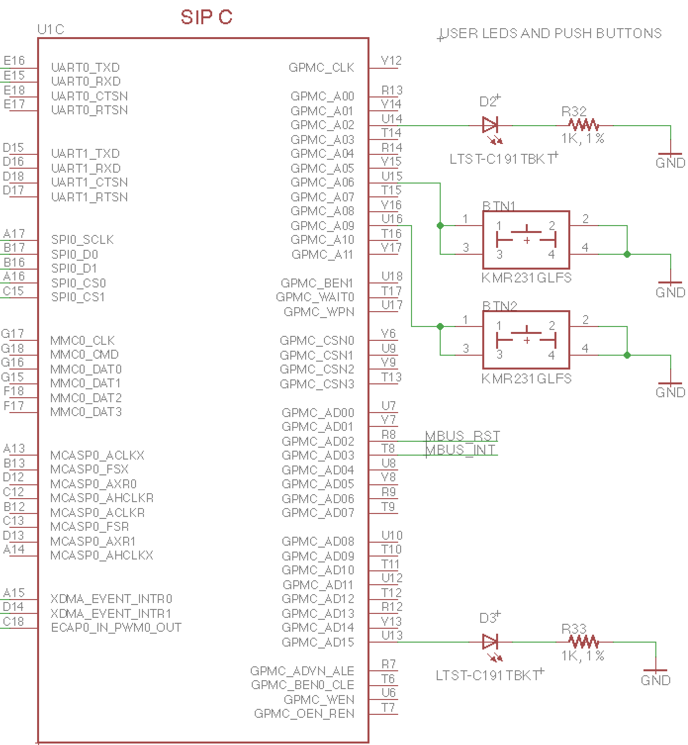
User Buttons and LEDs
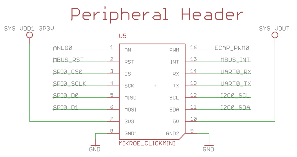
Peripheral Headers
References and Acknowledgments
- SO YOU WANT TO BUILD AN EMBEDDED LINUX SYSTEM?
- OSD335x-SM System-in-Package Smallest AM335x Module, Quickest Design
- OSD335x Reference Design Tutorial Series
Original: https://wiki-power.com/ This post is protected by CC BY-NC-SA 4.0 agreement, should be reproduced with attribution.
This post is translated using ChatGPT, please feedback if any omissions.