ESD Fundamentals
ESD (Electrostatic Discharge) refers to the rapid transfer of electrons that occurs when two objects come into close proximity or contact. It is a well-known phenomenon that objects can generate and accumulate electric charges through contact and friction with other objects. For instance, when our hands come into contact with external surfaces, they can accumulate a significant amount of positive charge. When an object with a substantial accumulation of positive charge is in close proximity to or in contact with a conductor, electrons will rapidly transfer from the conductor to the positively charged object. This rapid transfer of electrons is known as electrostatic discharge (ESD).
Electronic devices typically feature numerous interfaces connected to chips through wires, which in turn are connected to the internal components of the chips. The high voltages generated during electrostatic discharge (often reaching several kilovolts) can potentially puncture the wires and, in the case of high current, even damage the components. Therefore, it is crucial to prevent ESD.
The key to ESD protection is to provide a dedicated discharge path for electrostatic charges, similar in principle to a lightning rod. ESD protection devices are mainly categorized into four types: TVS diodes, varistors (MOV), MLCC (Multilayer Ceramic Capacitors), and ESD suppressors.
ESD Testing Models
| HBM | MM | CDM | IEC 61000-4-2 MODEL | |
|---|---|---|---|---|
| Test Voltage (V) | 500-2000 | 100-200 | 500-2000 | 2000-15000 |
| Pulse Duration (ns) | ~150 | ~80 | ~1 | ~150 |
| Peak Current at 2kV (\(A_{pk}\)) | 1.33 | - | ~5 | 7.5 |
| Rise Time | 25ns | - | <400ps | <1ns |
| Number of Voltage Impacts | 2 | 2 | 2 | 20 |
Human Body Model (HBM)
The HBM test simulates electrostatic discharge from the human body, replicating the scenario where a person touches a chip with their hand.
Machine Model (MM)
The MM test simulates electrostatic discharge from mechanical sources, imitating scenarios where chips experience ESD due to contact with mechanical tools or objects with lower resistance. The main difference from the HBM is the larger capacitance and absence of resistance, resulting in significantly higher discharge currents. Additionally, the inductance of the conductors can introduce oscillatory currents during chip discharge, causing alternating positive and negative current changes.
Charged Device Model (CDM)
The first two models simulate scenarios where charged objects discharge to the chip. In contrast, the Charged Device Model simulates situations where the chip itself becomes charged and discharges to the ground. This can occur when a chip is taken out of packaging that has been stored for some time. In this case, there is no resistance or capacitance, and the chip directly discharges to the ground through its pins.
ESD Reference Standards
Common HBM testing specifications include:
| Standard | Charging Capacitance \(C_d (pF)\) | Discharge Resistance \(R_d (Ω)\) |
|---|---|---|
| AEC-Q200-002 | 150 | 2000 |
| IEC61000-4-2 | 150 | 330 |
For example, the ESD HBM test circuit based on the AEC-Q200-002 standard is as follows:
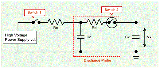
In this circuit, \(C_x\) represents the capacitance of the device under test, \(C_d\) is the charging capacitance, \(R_d\) is the discharge resistance, and \(R_c\) is the protection resistance. The ESD testing procedure is as follows:
- Switch 1 closed, Switch 2 open: High voltage power supplies charge \(C_d\) with electric charge.
- Switch 1 open, Switch 2 closed: The electric charge stored in \(C_d\) is applied to \(C_x\) for ESD testing.
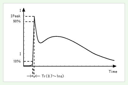
Discharge Current Curve:
ESD Test Procedure
Following the AEC-Q200-002 standard, the HBM test procedure can be performed as shown in the following diagram:
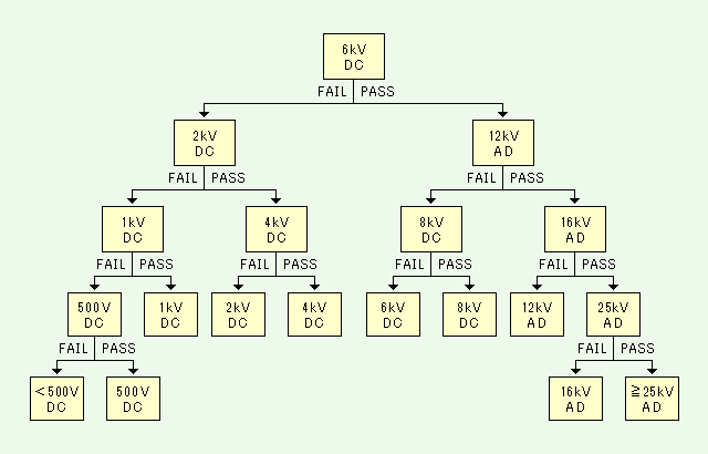
The voltage withstand levels determined through testing are categorized as follows:
| Classification | Maximum Withstand Voltage |
|---|---|
| 1A | Less than 500V (DC) |
| 1B | 0.5 kV (DC) or more, less than 1 kV (DC) |
| 1C | 1 kV (DC) or more, less than 2 kV (DC) |
| 2 | 2 kV (DC) or more, less than 4 kV (DC) |
| 3 | 4 kV (DC) or more, less than 6 kV (DC) |
| 4 | 6 kV (DC) or more, less than 8 kV (DC) |
| 5A | 8 kV (DC) or more, less than 12 kV (AD) |
| 5B | 12 kV (AD) or more, less than 16 kV (AD) |
| 5C | 16 kV (AD) or more, less than 25 kV (AD) |
| 6 | 25 kV (AD) or more |
DC (Direct Contact Discharge) refers to direct contact discharge, and AD (Air Discharge) refers to air discharge.
Relationship Between Capacitance Value of the Test Object and ESD Resistance
The capacitance value of the test object \(C_x\) affects the voltage at its two ends according to the following relationship:
When the power supply voltage (\(V_d\)) and charging capacitance (\(C_d\)) are constant, an increase in the capacitance value of the test object (\(C_x\)) results in a decrease in the voltage ($V_x) at its two ends.
Therefore, in general, as the capacitance value (\(C_x\)) increases, there is a trend for increased ESD resistance. However, in practice, due to differences in design factors such as the type and thickness of the dielectric, the performance range of voltage withstand also varies and does not entirely follow the trend mentioned above.
Capacitance Value and ESD Resistance Reference
- \(C_x\) capacitance parameters: GCM series / 0402 package / X7R / 50V
- Test conditions: \(C_d=150pF, R_d=2kΩ\)
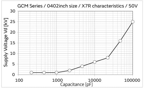
From the graph, it can be seen that to withstand 1kV ESD, a 1000pF capacitor can be used for protection. In actual circuit design, it's advisable to parallel a large resistor with the capacitor to discharge the electric charge stored in the capacitor after eliminating ESD.
References and Acknowledgments
- Introduction to Reliability and ESD
- EE Engineer's Notebook: Basic ESD Knowledge and ESD Protection Selection
- ESD Resistance of Capacitors
- Understanding the Role of ESD Devices in PCB Design
Certainly, here's the translation of the provided text into English:
This post is translated using ChatGPT, please feedback if any omissions.