Basics of ADC and DAC
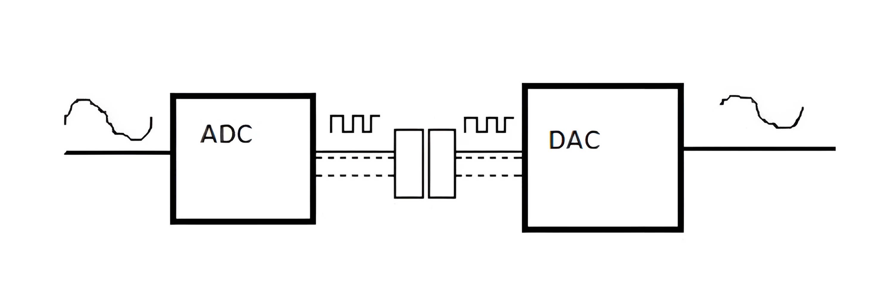
In the real world, most common signals are analog, such as temperature, sound, and pressure. However, in signal processing and transmission, digital signals are often used to reduce noise interference. Therefore, we frequently convert real-world analog signals into digital signals through ADC for computation, transmission, and storage, and then convert them back to analog signals using DAC for presentation.
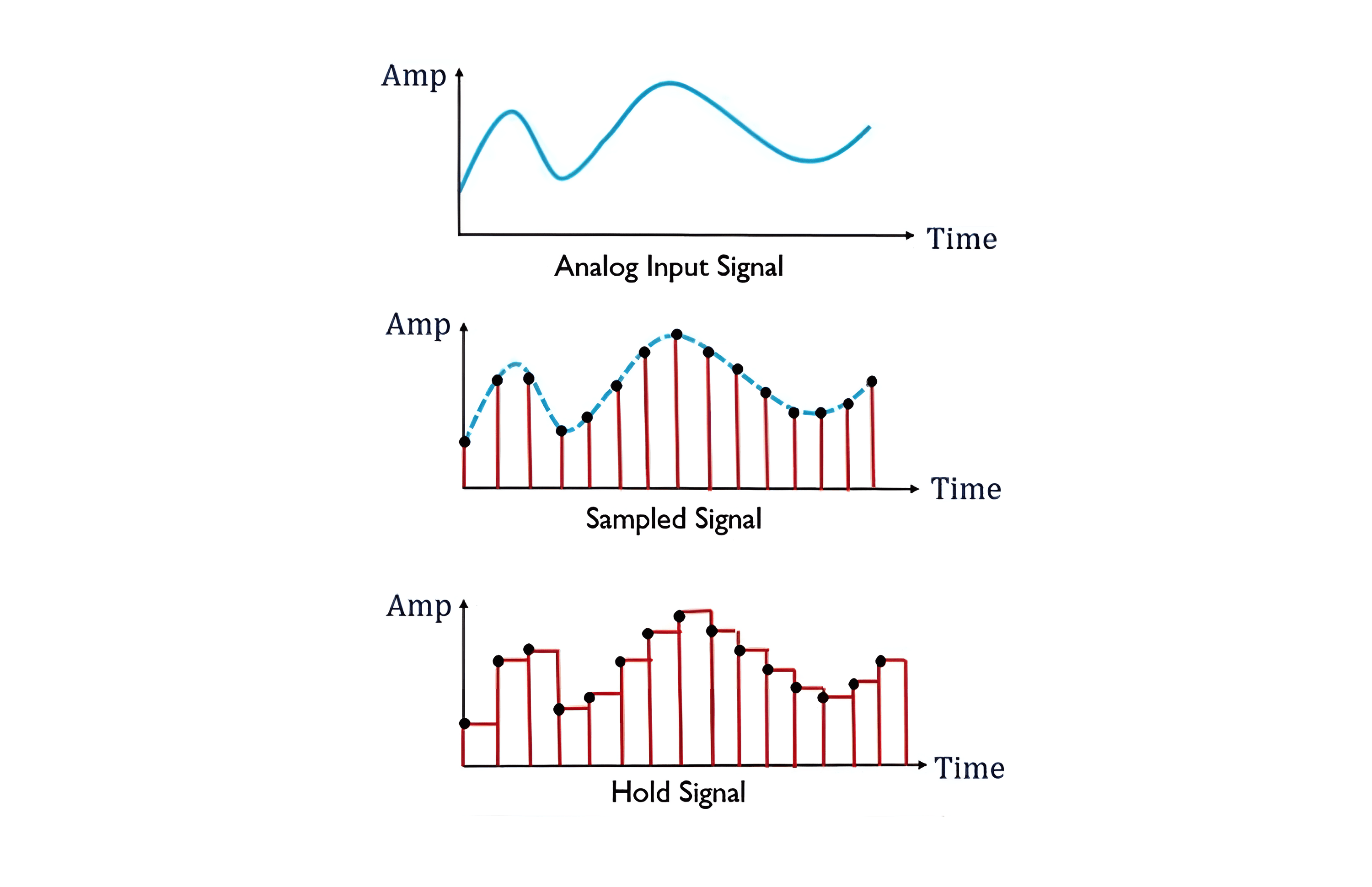
It's important to note that analog signals in the real world are continuous, meaning they have infinite resolution. However, when converted into digital form, a certain level of precision is lost, and both time and amplitude become discrete values.
Basic Principles of ADC
ADC, which stands for Analog-to-Digital Converter, is a device that converts real-world analog signals like temperature, pressure, sound, or images into a digital form that's easier to store, process, and transmit.
Sampling
Since the input analog signal is continuous, and the desired output is discrete, we can only perform instantaneous sampling. The sampled values are then converted into digital quantities, and the process repeats for the next round of sampling.
To accurately represent the analog input signal \(v_1\) with the signal \(v_s\), we need to satisfy the Nyquist sampling theorem. This means that the sampling frequency \(f_s\) should be at least twice the maximum frequency component \(f_{i(max)}\) of the analog input signal (typically, 3-5 times is chosen, but very high frequencies require faster operation, considering cost):
As long as the Nyquist theorem is satisfied, a low-pass filter can be used to restore \(v_s\) to \(v_1\). The filter voltage transfer function should remain constant for frequencies below \(f_{i(max)}\) and rapidly decrease to zero before \(f_s-f_{i(max)}\).
Holding
A holding circuit allows the signal to be maintained for a certain duration after sampling, giving the ADC enough time to perform the conversion. Generally, the higher the sampling pulse frequency and the denser the sampling, the more sampled values are obtained, and the output signal of the sample-and-hold circuit will closely resemble the waveform of the input signal. The basic form of a sample-and-hold circuit is as follows:
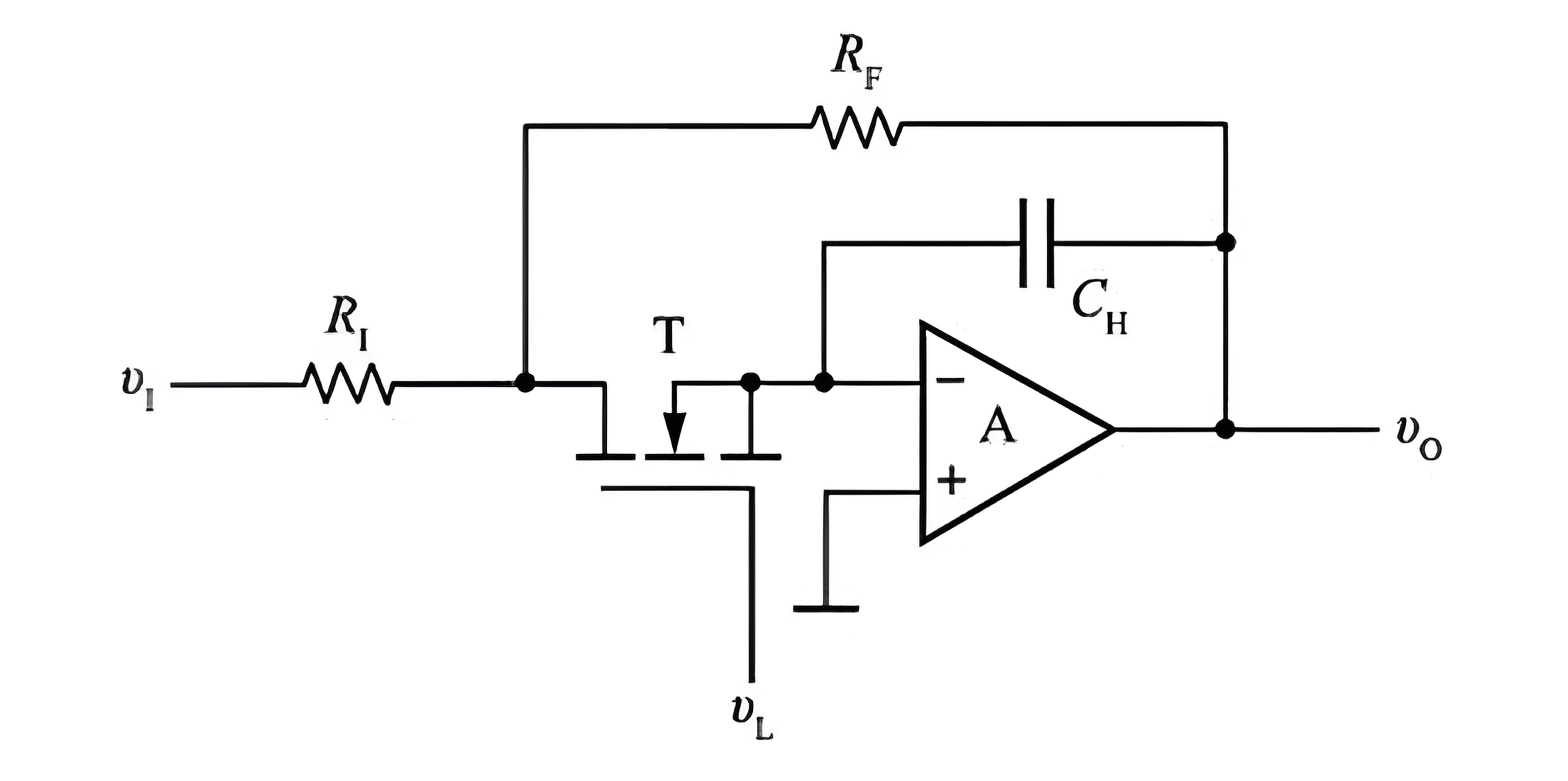
The basic steps of sample and hold are:
- When the sampling control signal \(v_L\) is high, MOS transistor \(T\) is turned on, and \(v_1\) charges the capacitor $C_H" through resistor \(R_1\) and MOS transistor \(T\).
- If \(R_1=R_F\), then after charging, \(v_0=v_c=-v_1\).
- When the sampling control signal \(v_L\) falls back to a low level, MOS transistor \(T\) turns off, and the voltage on capacitor \(C_H\) does not change suddenly, so \(v_0\) can be maintained for a period, allowing the sampling result to be recorded.
Quantization
The digital quantity obtained through sampling must be an integer multiple of a specified minimum unit value. This process is called quantization, and the minimum unit value is known as the quantization unit Δ. The magnitude represented by the least significant bit (LSB) of the digital signal is equal to Δ.
Because analog voltage is continuous, it may not be divisible by Δ, resulting in quantization error.
The finer the quantization level, the smaller the quantization error, but it requires more binary bits, making the circuit more complex.
Encoding
The quantized result is represented in binary (or another base), which is known as encoding.
Common Types of ADC
Parallel Comparator (Flash)
The parallel comparator ADC, also known as Flash ADC, belongs to the direct ADC category. It directly converts the input analog voltage into digital output without any intermediate variable conversion. It consists of a series of voltage comparators, each of which compares the input signal with a unique divided reference voltage. The outputs of the comparators are connected to the input of the encoder circuit, generating binary output.
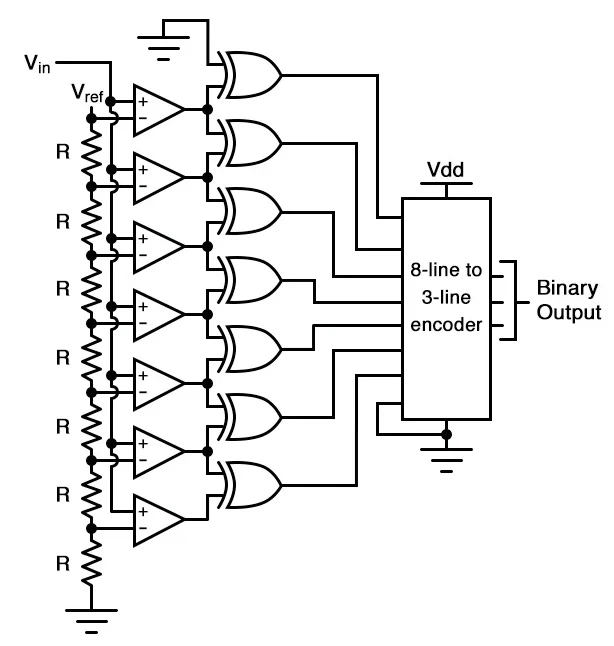
Not only is it the simplest in terms of operational theory, but it is also the most efficient in terms of speed, limited only by the comparator and gate propagation delays. Unfortunately, for any given number of output bits, it is the densest component.
The fastest conversion speed is achieved by the parallel comparative type ADC, but its drawback lies in the requirement for numerous voltage comparators and large-scale code conversion circuits (commonly used parallel comparative outputs are mostly below 8 bits).
Successive Approximation Type
The Successive Approximation ADC employs a feedback comparative circuit structure composed of comparators, DAC, registers, clock pulse source, and control logic, as shown below:
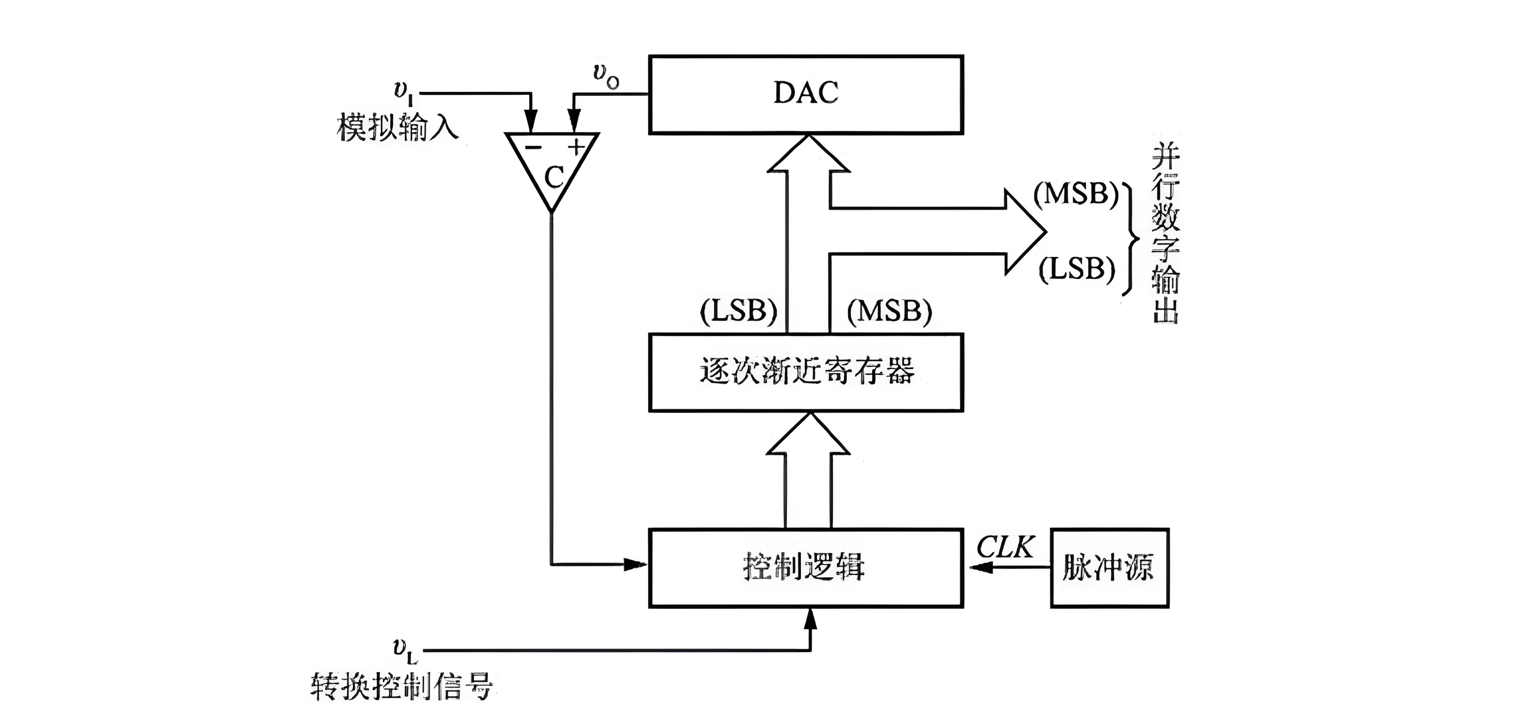
The principle involves setting a digital value and obtaining a corresponding analog voltage output via the DAC. This analog voltage is sequentially compared to the input analog voltage signal starting from the highest bit. If they are not equal, the digital value is adjusted until the two analog voltages are equal. The final digital value obtained is the desired conversion result. This process is akin to weighing an object's position and weight using a balance, starting with larger weights and successively adding or replacing smaller weights.
The advantages of the Successive Approximation ADC include high speed, low power consumption, and cost-effectiveness at low resolutions (12 bits). However, its drawback is the average conversion rate and moderate circuit size.
Dual Integration Type (V-T)
The Dual Integration ADC is an indirect ADC that first converts the input analog voltage signal into a time-width signal directly proportional to it. Within this time width, a fixed-frequency clock is counted, and the count value represents the digital signal proportional to the analog input voltage. Therefore, this type of ADC is also referred to as the Voltage-Time Transformation (V-T) ADC.
The Dual Integration ADC is composed of integrators, comparators, counters, control logic, and a clock signal source, as illustrated below:
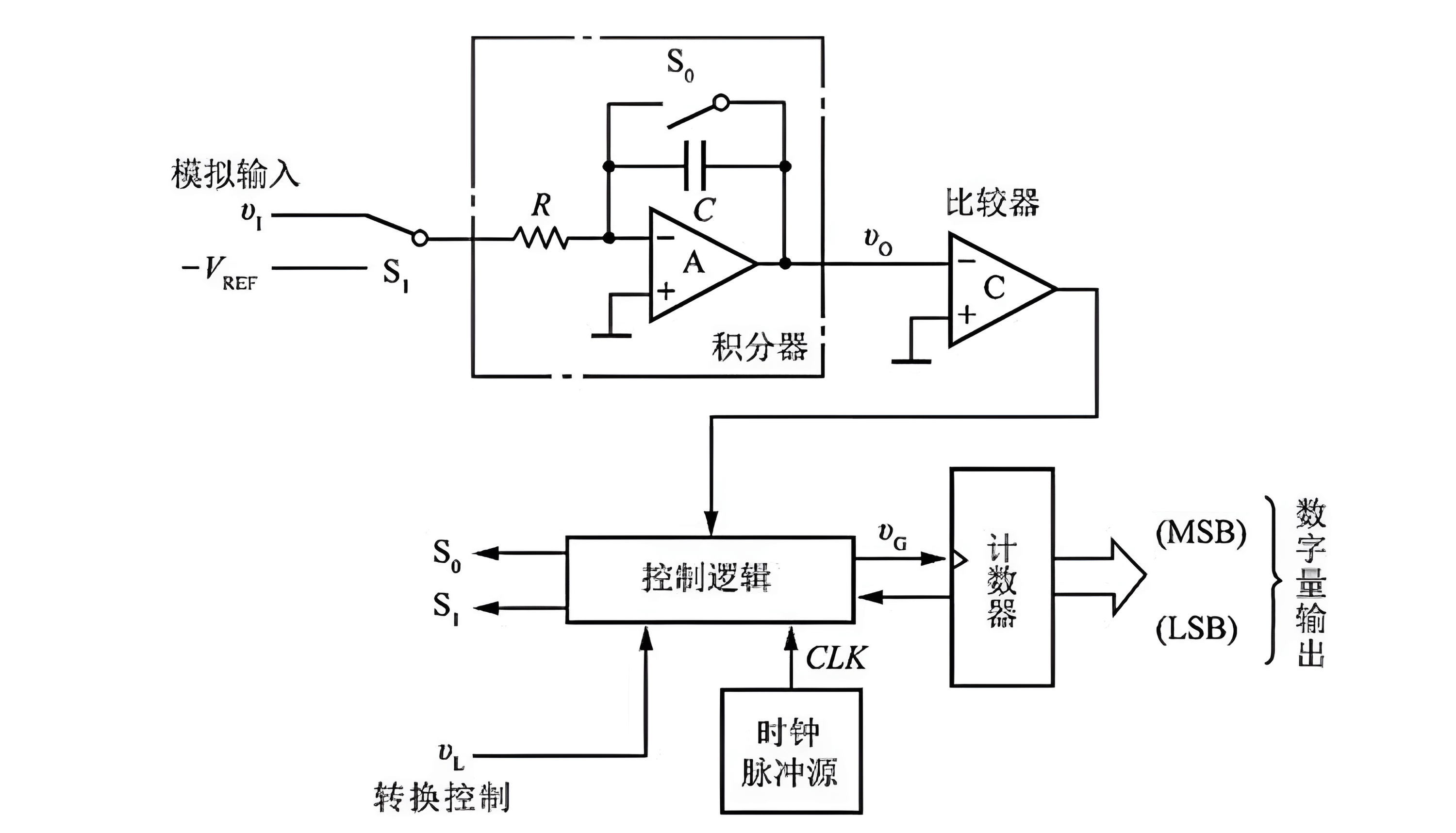
The advantages of the Dual Integration ADC are stable performance (due to double integration, eliminating differences in RC parameters) and strong resistance to interference (minimal impact from noise on the integration process). However, its drawback is the low conversion rate (conversion accuracy depends on integration time).
Σ-Δ Type
The Σ-Δ Modulation ADC operates on a principle distinct from parallel and successive approximation ADCs mentioned earlier. Instead of quantifying and encoding the absolute value of the sampled signal, it quantifies and encodes the difference (increment) between two consecutive sampled values. Its basic structure is depicted below:
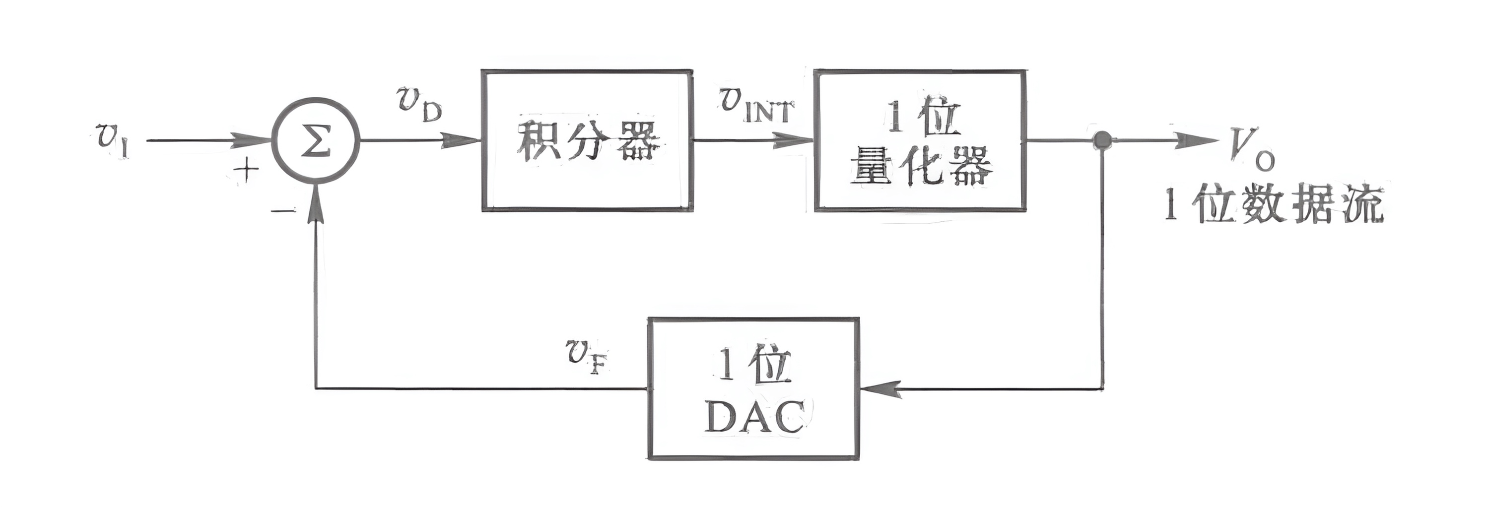
It consists of a linear voltage integrator, a 1-bit output quantizer, a 1-bit input DAC, and a summation circuit. The quantized output signal \(V_0\) is converted to an analog signal \(V_F\) through the DAC and fed back to the input summation circuit. This feedback is subtracted from the input signal \(v_1\) to yield the difference \(v_D\). The integrator linearly integrates $v_D," generating an output voltage \(v_{INT}\) for the quantizer, which quantizes it into a 1-bit digital output. Because it employs a 1-bit output quantizer, the output signal \(V_0\) in continuous operation is a data stream composed of 0s and 1s.
The Σ-Δ Modulation ADC's advantages include achieving high-resolution measurements with ease. However, its drawbacks are a low conversion rate and a large circuit size.
Voltage-Frequency Transformation Type (V-F)
The Voltage-Frequency Transformation (V-F) ADC is another indirect ADC consisting mainly of a V-F converter (also known as a Voltage Controlled Oscillator, VCO), a counter with its clock signal control gate, registers, and a monostable trigger, as shown here:
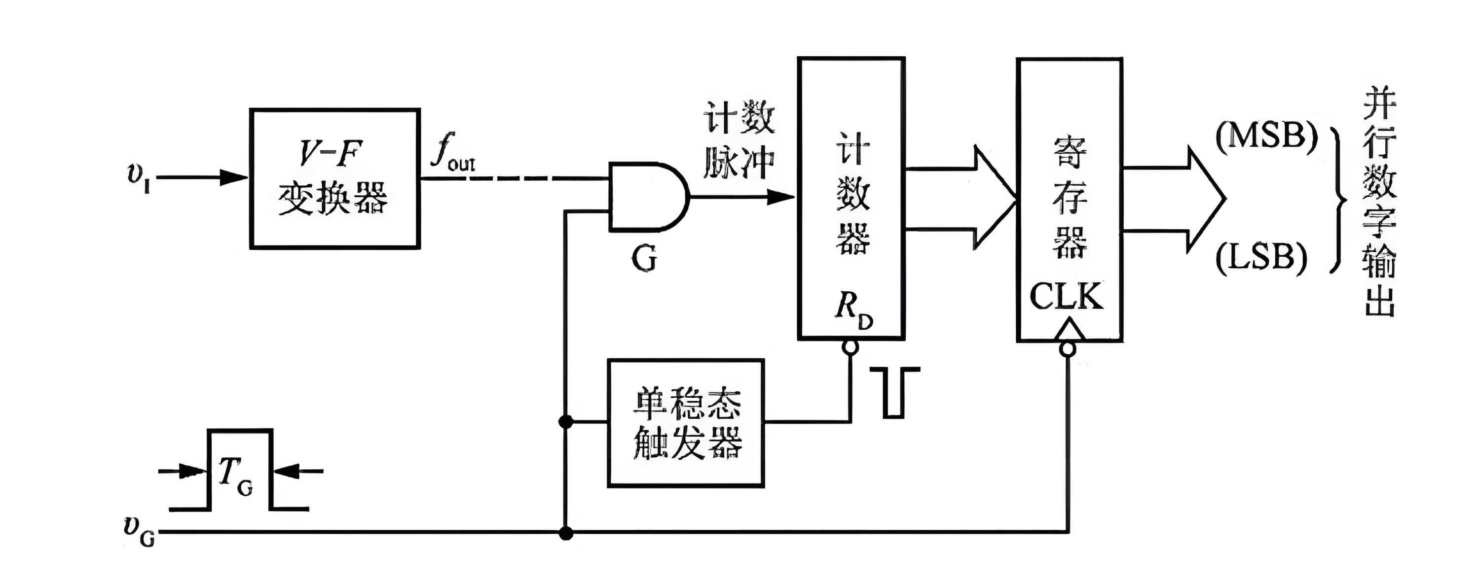
The principle involves:
- Converting the input analog voltage signal into a corresponding frequency signal.
- Counting the frequency signal over a fixed time period.
- The count result is proportional to the amplitude of the input voltage.
Key ADC Parameters
- Resolution: The resolution refers to the change in analog voltage that is required to produce a one-unit change in the digital output. It is typically represented in binary bits, where a resolution of 'n' means it is one part in 2^n of the full scale 'Fs'.
- Quantization Error: It is the error introduced when quantizing an analog signal with a finite number of bits in an ADC. To accurately represent analog signals, the number of bits in the ADC would need to be very large, or even infinite, which is not practical. Thus, all ADC devices have quantization errors. The quantization error is the maximum deviation between the step-like conversion characteristic curve of a finite-resolution ADC and the conversion characteristic curve of an ADC with infinite resolution.
- Conversion Rate: The number of conversions performed per second.
- Conversion Range: The maximum voltage that an ADC can measure, which is generally equal to the reference voltage. Exceeding this voltage can potentially damage the ADC. When dealing with smaller signals, it's possible to reduce the reference voltage to enhance resolution. However, altering the reference voltage will also change the corresponding conversion values. Therefore, it's important for the reference voltage to be stable and free from high-order harmonics.
- Offset Error: When the ADC input signal is zero, but the ADC conversion output signal is not zero, there is an offset error.
- Full-Scale Error: The difference between the input signal corresponding to the full-scale output of the ADC and the ideal input signal value.
- Linearity: The maximum deviation of the actual transfer function of an ADC from an ideal straight line.
Basic Principles of DAC
DAC (Digital-to-Analog Converter) is a device that converts digital data into proportional analog voltage or current. For example, a computer might generate digital output ranging from 00000000 to 11111111, and a DAC converts this into a voltage ranging from 0 to 10V. DACs can be broadly categorized into two types based on their basic principles: current summing type and voltage divider type.
Common Types of DACs
Switched Resistor Type
The switched resistor DAC is the simplest type of DAC, consisting of a resistor voltage divider and a tree-like network of switches:
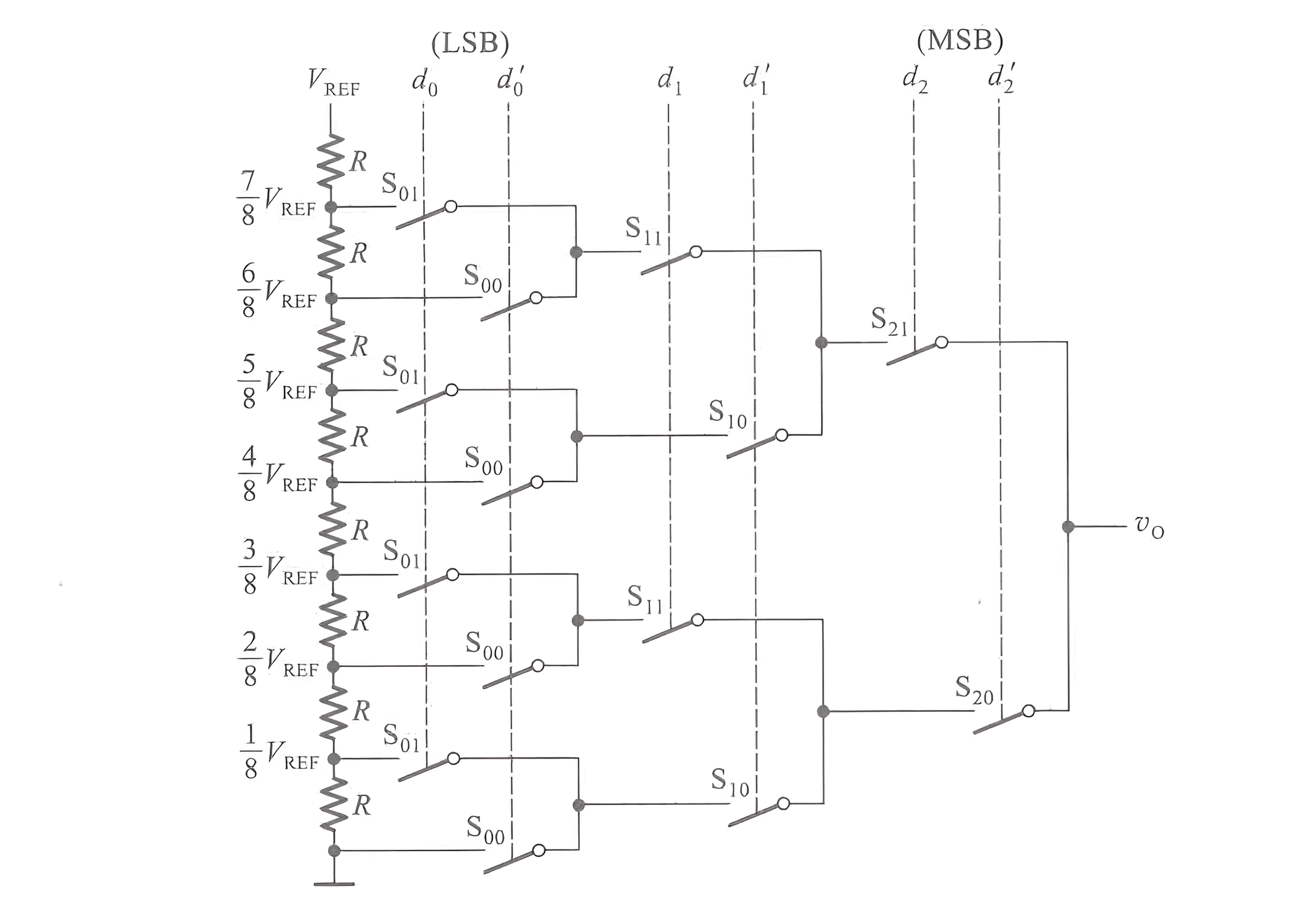
These switches are controlled by 3-bit inputs \(d_0, d_1, d_2\), and the output is calculated as follows:
Furthermore, for an n-bit binary input in the switched resistor DAC, the output is given by:
The switched resistor DAC is characterized by its use of a single type of resistor and does not require high switch conduction resistance at the output. However, it has the drawback of using many switches.
Weighted Resistor Network
The term "weight" refers to the value that each 1 in a multi-bit binary number represents. For example, in an n-bit binary number \(D_n = d_{n-1}d_{n-2}\ldots d_1 d_0\), the weights from the most significant bit (MSB) to the least significant bit (LSB) are \(2^{n-1}, 2^{n-2}, \ldots, 2^1, 2^0\).
The principle of the weighted resistor network type DAC (which belongs to the voltage output type) is illustrated in the diagram below (4 bits). It consists of a weighted resistor network, four electronic switches, and a summing amplifier:
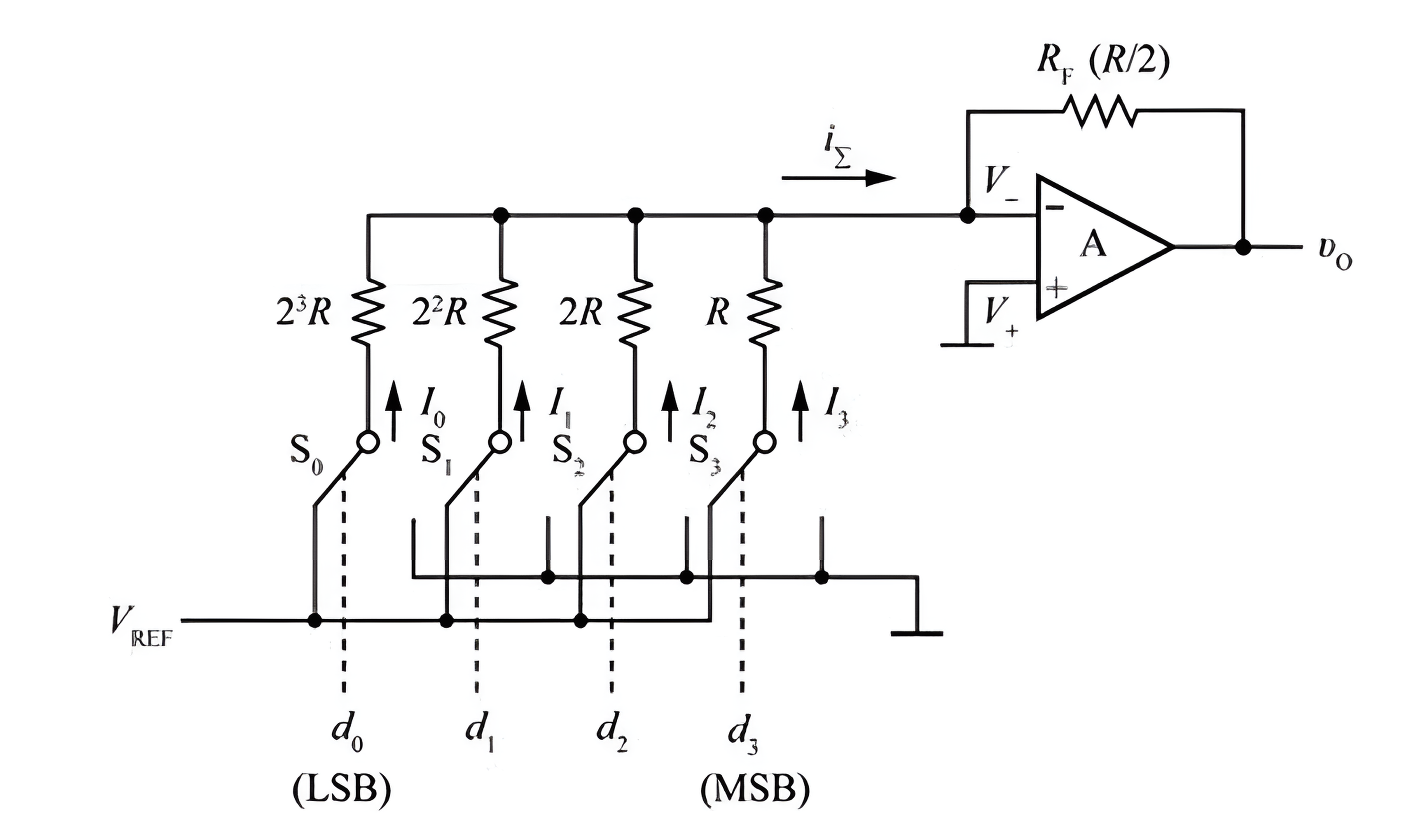
Here, \(S_0, S_1, S_2, S_3\) are four electronic switches controlled by signals \(d_0, d_1, d_2, d_3\). When the input is 1, the switch connects to \(V_{REF}\); when the input is 0, the switch connects to ground. Thus, when \(d_i = 1\), a current \(I_i\) flows to the summing amplifier, and when \(d_i = 0\), the current is zero. The summing amplifier is a negative feedback amplifier, and its output voltage \(v_0\) is positive when the inverting input \(V_-\) is lower than the non-inverting input \(V_+\). When \(V_- > V_+\), \(v_0\) is negative. Furthermore, when \(V_-\) is slightly higher than \(V_+\), a significant negative output voltage is generated in \(v_0\). \(v_0\) is fed back through \(R_F\) to reduce \(V_-\) back to \(V_+\) (0V).
Assuming the operational amplifier is an ideal device (with zero input current), we can derive the following:
Additionally, since \(V_-\approx 0\), the individual branch currents are as follows:
Here, \(d_n\) can be either 0 or 1. Substituting into the previous equation and assuming the feedback resistance \(R_F=\frac{R}{2}\), we can obtain the output voltage as:
Furthermore, for an n-bit weighted resistor network DAC with feedback resistance \(R_F=\frac{R}{2}\), the output voltage calculation formula becomes:
Hence, the analog output voltage is proportional to the digital input quantity \(D_n\), and its range varies from 0 to \(-\frac{2^n-1}{2^n}V_{REF}\). On the other hand, if a positive output voltage is required, a negative \(V_{REF}\) should be provided.
The advantage of a weighted resistor network DAC is its simple structure, but the drawback is that resistor values can differ significantly, leading to potential accuracy issues in practice. To improve this, a bipolar weighted resistor network can be used, which is not detailed here but still does not fundamentally solve the problem.
Inverted T-Resistor Network
To address the issue of widely varying resistor values in a weighted resistor network DAC, an inverted T-resistor network DAC, also known as R2R DAC, can be used. It uses only two resistor values: R and 2R, which greatly improves control accuracy:
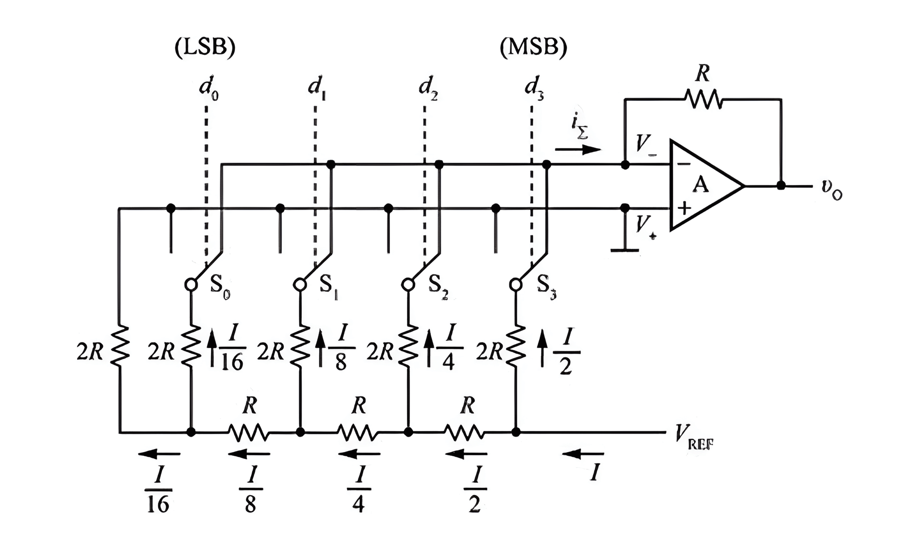
When the feedback resistor of the summing amplifier has a resistance of R, the output voltage is given by:
It is evident that the calculation formula for the inverted T-resistor network is the same as that for the weighted resistor network DAC.
Current-Weighted Type
In the analysis of the weighted resistor network and inverted T-resistor network, analog switches are treated as ideal devices. However, in reality, they have some on-resistance and voltage drop, and there are inconsistencies in switch performance. This can lead to conversion errors affecting accuracy. The solution is to use a current-weighted DAC, which has a set of constant current sources. The current of each source is half of the previous one and is proportional to the binary weight of the input.
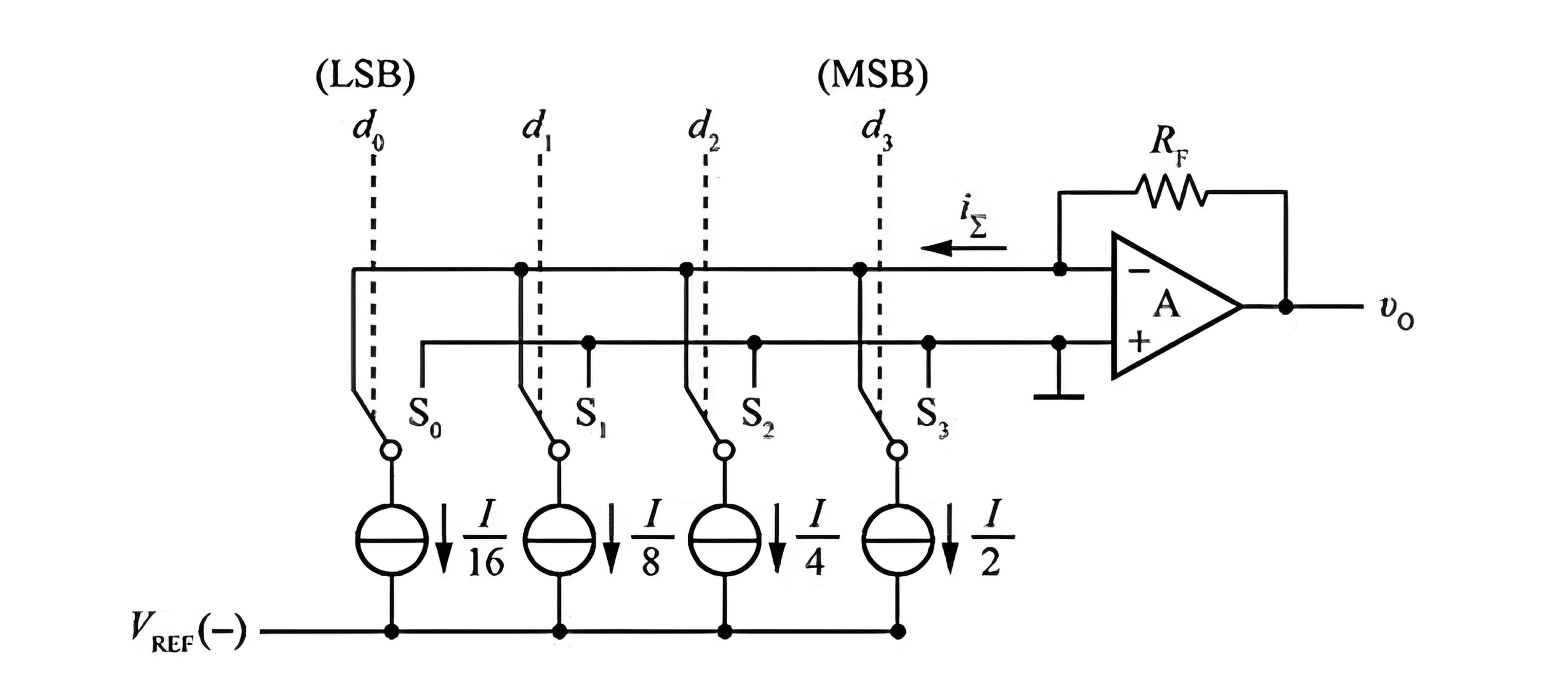
When a certain bit of the input digital value is 1, the corresponding switch connects the constant current source to the input of the operational amplifier. When the input code is 0, the switch is grounded, resulting in an output voltage of:
Key DAC Parameters
- Resolution: The ratio of the smallest output voltage (corresponding to an input digital value of 1) to the largest output voltage (corresponding to an input where every bit is 1). Typically represented by the number of bits in the input digital value.
- Conversion Range: The maximum voltage that the DAC can output, often related to the reference voltage or its multiples.
- Settling Time: The delay time from the input digital value to the analog output.
- Conversion Accuracy: Similar to ADC's conversion accuracy.
References and Acknowledgments
- "ADC/DAC Application Design Compendium"
- "Analog-to-Digital and Digital-to-Analog Conversion"
- "ADC and DAC (Analog to Digital And Digital to Analog Converters)"
- "Exploring the Principles of DAC"
- "Analog Engineer’s Pocket Reference"
- "Digital Electronics Technology (6th Edition) by Yan Shi"
Original: https://wiki-power.com/ This post is protected by CC BY-NC-SA 4.0 agreement, should be reproduced with attribution.
This post is translated using ChatGPT, please feedback if any omissions.