Design of Reverse Connection Protection Circuit
Reverse connection protection circuit is quite important in circuit design because you never know what kind of tricky operations your users might perform, which could lead to a board explosion due to reverse connection of the power supply. A good reverse connection protection circuit, at the cost of adding a few more components, ensures the safety and responsibility towards the users/products.
Diode Reverse Connection Protection Circuit
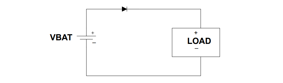
As shown in the diagram, a diode (unidirectional conductivity) is added in the positive/negative path of the power supply to achieve reverse connection protection. This circuit is simple and has the lowest cost. The disadvantages are high voltage drop (around 0.6V), more severe heating with higher current, and leakage current when the reverse voltage is too high, so a sufficient margin should be left. Schottky diodes with relatively higher cost but lower voltage drop can be chosen.
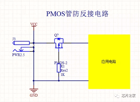
;## P-MOS Tube Reverse Connection Protection Circuit
;
;
;
;Taking the above diagram as an example, when the power is just turned on, the parasitic diode of the MOS tube conducts, and the voltage at the S level is VCC-0.6V, while the G level is 0V, causing the P-MOS to conduct. When the power supply is reversed, the G level is at a high level and does not conduct, thus protecting the subsequent stage.
;
;In practical applications, a resistor can be added between the gate and source of the P-MOS. This method also has a distinction between P-MOS and N-MOS, both of which utilize the parasitic diode and its conductivity of the MOS tube. However, the conduction resistance of N-MOS is smaller than that of P-MOS, so it slightly reduces power consumption. After the power supply is reversed, the MOS tube becomes an open circuit, effectively protecting the subsequent circuit. This method is widely used, and it is recommended to use N-MOS in practice.
MOSFET Reverse Connection Protection
MOSFET has a lower on-resistance (\(R_{DS(on)}\)) and can be used as a reverse connection protection circuit with only a small power loss. Since N-MOS conducts at a high level of G and P-MOS conducts at a low level of G, N-MOS is generally used for reverse connection protection on the low-end side, while P-MOS is used on the high-end side:


When the power supply is correctly connected, the MOS tube conducts and the subsequent circuit can receive power normally. When the power supply is reversed, the MOS tube cuts off, disconnecting to protect the subsequent circuit.
The loss of MOSFET reverse connection protection is \(R_{DS(on) * I_{load}}\). The selection criteria for MOSFET are to minimize \(R_{DS(on)}\) and ensure \(U_{GS(th)}\) is below the power supply voltage. Compared to P-MOS, N-MOS has a smaller conduction resistance and a wider range of options.
Rectifier Bridge Reverse Connection Protection Circuit
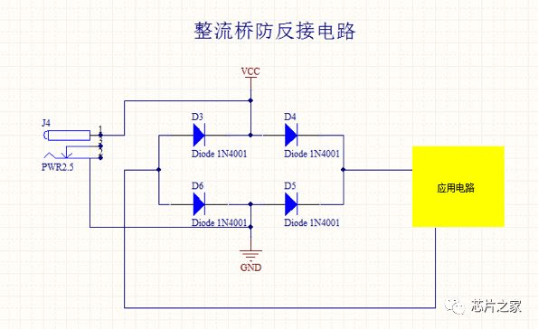
The bridge rectifier circuit has two diodes that cause voltage drop and have relatively large power consumption and heat generation. Unless in special circumstances, it is generally not recommended to use this circuit.
Fuse + Voltage Regulator Diode
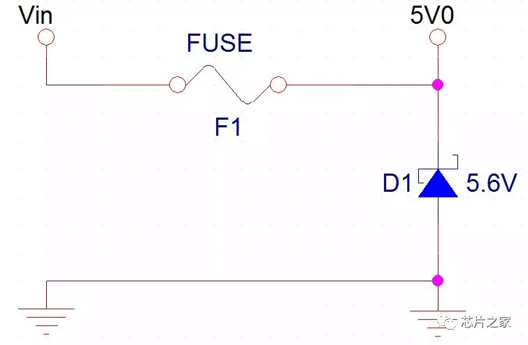
This circuit design is very clever as it provides both reverse connection protection and overvoltage protection. The principle is as follows:
When the power supply Vin is reversed, the voltage regulator diode D1 conducts in the forward direction, and the negative voltage across the load is the forward voltage drop Vf of the diode. Usually, Vf is relatively low and will not burn out the subsequent load circuit. At the same time, the voltage mainly drops across F1, so the current will rapidly increase until it exceeds the fuse current, causing the fuse to blow and disconnect the power supply. This prevents D1 from being damaged due to excessive current.
When the voltage is positive but exceeds the voltage of the voltage regulator diode (e.g., greater than 5.6V), the load end receives a voltage of approximately 5.6V due to the presence of the voltage regulator diode D1. However, there will be a relatively high voltage (Vin-5.6V) across F1, causing the current to increase until the fuse blows, protecting the backend circuit. This is the overvoltage protection.
There are a few points to note about this circuit:
Translate into English:
- Selection of fuses. The rated current of the fuse should be greater than the normal operating current of the downstream load (the fuse should not blow during normal circuit operation).
- Selection of voltage regulator diodes. The voltage rating of the diode should be higher than the normal input voltage (the diode should not break down during normal power supply input), but lower than the maximum allowable input voltage of the downstream circuit (the diode should not burn out the downstream circuit).
- The condition
maximum allowable current of the voltage regulator diode + load current during power-on > breakdown current of the fuseshould be satisfied. Only when the fuse is blown before the power supply overvoltage input, the voltage regulator diode will not burn out due to excessive current passing through. - The negative voltage Vf generated in reverse connection circuits is generally less than 1.5V. The backend circuit should be able to withstand a negative voltage of 1.5V without being damaged.
- This circuit should be used in circuits with a power less than 500mW as much as possible.
References and Acknowledgements
- Have you mastered these 4 commonly used reverse connection circuits?
- Reverse Current/Battery Protection Circuits
This post is translated using ChatGPT, please feedback if any omissions.