Power Supply Design - Non-Isolated Switching Regulator IC
Factors to Consider in Design
The design of a switching power supply should take into account the following conditions:
- Input/Output Voltage: Select within the recommended operating voltage range of the device, considering the range of actual voltage fluctuations, ensuring compliance with device specifications.
- Output Current: Allow for a margin in the output current and evaluate the momentary peak current and heating conditions of the circuit, meeting derating requirements.
- Ripple: Ripple is an important parameter measuring the output voltage fluctuation of the circuit. Pay attention to light load and heavy load ripple. Typically tested with an oscilloscope with a 20 MHz bandwidth.
- Efficiency: Pay attention to both light and heavy load conditions. Light load affects standby power, while heavy load affects temperature rise. Usually, for a 12V input and 5V output at 10mA, efficiency should be above 80%.
- Transient Response: Transient response characteristics indicate whether the system can adjust promptly to ensure stable output voltage when the load changes rapidly. A smaller output voltage fluctuation is better, typically requiring less than 10% peak-to-peak.
- Switching Frequency: Typically above 500 kHz, it relates to the choice of inductance and capacitance, and other issues such as EMC and noise under light load.
- Feedback Reference Voltage and Precision: Compare the feedback voltage with the internal reference voltage and use external feedback divider resistors to obtain different output voltages. Different products may have different reference voltages, such as 0.6-0.8V, and feedback resistors should have a 1% accuracy.
- Line Regulation and Load Regulation: Line regulation reflects the stability of the output voltage with input voltage variation, while load regulation reflects the stability of the output voltage with output load variation. Generally, 1% is required, with a maximum not exceeding 3%.
- EN Voltage Level: EN high and low levels must meet device specifications; some ICs cannot exceed specific voltage ranges. Due to timing control requirements, this pin may have added capacitance, so ground resistance is necessary for level adjustment and discharge shutdown.
- Protection Performance: Overcurrent protection (OCP), over-temperature protection (OTP), and the ability to self-recover after protection conditions cease.
- Other Requirements: The project must have soft start, consider thermal resistance and packaging, and ensure the temperature range can cover both high and low temperatures.
Selection Principles: Universality, cost-effectiveness, ease of procurement, long lifecycle, compatibility, and substitutability, derating, ease of production, and standardization.
Modulation Methods
PFM (Pulse Frequency Modulation)
The switch pulse width remains constant, but the output voltage stability is achieved by changing the pulse output frequency. It is suitable for long-term use, especially with light loads, as it has the advantage of low power consumption.
PWM (Pulse Width Modulation)
The frequency of switch pulses remains constant, but the output voltage stability is achieved by changing the pulse width. It offers high efficiency and has lower ripple and noise.
Can Ground Copper Be Laid at the Bottom of the Power Inductor?
From an EMI perspective, it is advisable to lay copper; from the perspective of inductance, for shielded inductors, the inductance is basically unaffected, so copper is also recommended; for E-shaped inductors, copper has a slight effect on inductance, and it can be decided based on the specific situation.
Determining Saturation of the Inductor
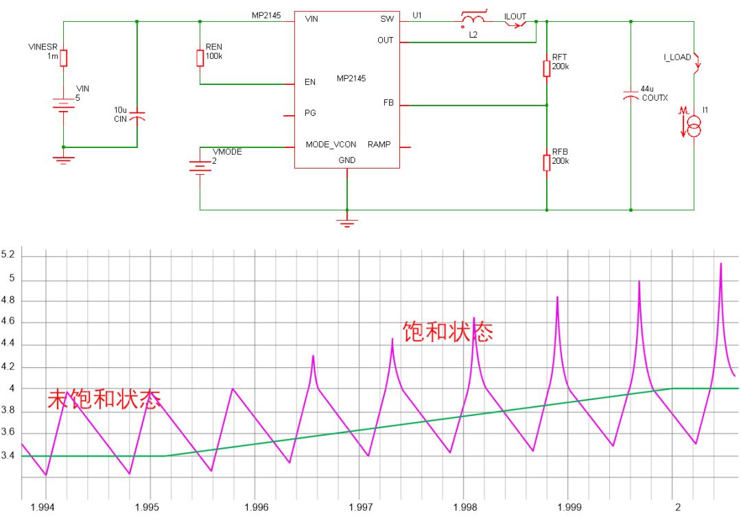
Apart from this, saturation can also be determined by abnormal temperature rise and whining.
Requirements for the Selection of Peripheral Components
- Input/Output Capacitors: Need to meet voltage resistance (1.5-2 times the input voltage) and input ripple requirements.
- BST Capacitor: Bootstrap startup capacitor, used to boost the voltage to turn on the upper switch inside the chip. Generally, follow the recommended values in the datasheet (usually 0.1-1uF), and the voltage resistance should generally be higher than the input voltage.
- Inductor: The required inductance varies for different output voltages; pay attention to temperature rise and saturation current to meet margin requirements, generally 1.3 times the maximum current (or the inductor saturation current must be greater than the maximum output current + 0.5 * inductor ripple current).
- Feedback Capacitor: Take the value as per the datasheet requirements; different chip manufacturers have different values, and different output voltages also have different requirements.
- Feedback Resistors and EN Divider Resistors: The values should be taken according to the datasheet, with a 1% accuracy required.
Switching Power Supply Ripple Analysis
🚧
PCB Layout Requirements
- Inductors: It is advisable to prioritize integrated inductors, as they exhibit lower electromagnetic interference (EMI).
- Feedback Network: The feedback traces should be routed as far away as possible from the inductors and power source noise. While meeting the first condition, you can also keep the traces short and thick, if possible. Ideally, these traces should be on the opposite side of the PCB relative to the inductors and should be separated by a ground plane in between. Voltage-divider resistors are usually connected to the signal ground (AGND), and feedback traces can be grounded.
- Decoupling Capacitors: Input decoupling ceramic capacitors should be placed as close as possible to the \(V_{IN}\) and GND of the chip to minimize parasitic inductance. You can add vias to the negative terminal of the capacitor to reduce impedance. Typically, larger electrolytic capacitors are needed at the front end of the power supply, and the power input should first go through a large capacitor and then a small one.
- Power Circuits should be short and thick, with a minimal loop area to reduce noise radiation. Keep the inductor close to the SW pin and away from the feedback traces. Output capacitors should be close to the inductor, and ground should have additional vias.
- BST Capacitor traces should be short and not too thin.
- Chip heatsinking should be done according to the design requirements, and additional vias for heat dissipation should be added underneath.
References and Acknowledgments
- In-depth Explanation of Three Basic Switching Power Supply Topologies (Chinese)
- Mastering these Techniques for Easy Operation of DC-DC Circuits (Chinese)
- MPS: Is it Violating Rules to Have a Ground Plane Underneath the Inductor? (Chinese)
- MPS Power Supply Classroom Episode 3: Tips for Judging Inductor Saturation (Chinese)
- How to Choose an Inductor for Buck Converters (Chinese)
- AN-1149 Layout Guidelines for Switching Power Supplies (English)
- Switching Power Supply Ripple Analysis (Chinese)
Original: https://wiki-power.com/ This post is protected by CC BY-NC-SA 4.0 agreement, should be reproduced with attribution.
This post is translated using ChatGPT, please feedback if any omissions.