Power Solution (Buck) - LMR14050
LMR14050 is a Buck converter chip from TI. It has a wide input voltage range (4-40V) and can provide a continuous output current of 5A. It has a sleep mode for light loads to improve efficiency. Due to its high level of integration, it requires very few peripheral components in the design. The switching frequency can be selected within the range of 200kHz-2.5MHz using an external resistor \(R_T\), or it can be synchronized with an external clock within the frequency range of 250kHz-2.3MHz. The protection features include thermal shutdown, output overvoltage protection (OVP), input undervoltage lockout (UVLO), cycle-by-cycle current limit, and short-circuit protection with frequency foldback.
Project Repository: Collection_of_Power_Module_Design/DC-DC(Buck)/LMR14050
Project Online Preview:
Key Features
- Topology: DC/DC (Buck)
- Device Model: LMR14050SDDA
- Package: HSOIC-8
- Input Voltage: 4-40V
- Output Voltage: 0.8-28V
- Output Current: 5A continuous
- Operating Frequency: 200kHz-2.5MHz
- Reference Price: ¥11.3
- Other Features
- 40µA ultra-low operating quiescent current
- Shutdown current: 1µA
- 90mΩ high-side MOSFET
- Minimum on-time: 75ns
- Current mode control
- Thermal protection, overvoltage protection, and short-circuit protection
Internal Functional Block Diagram
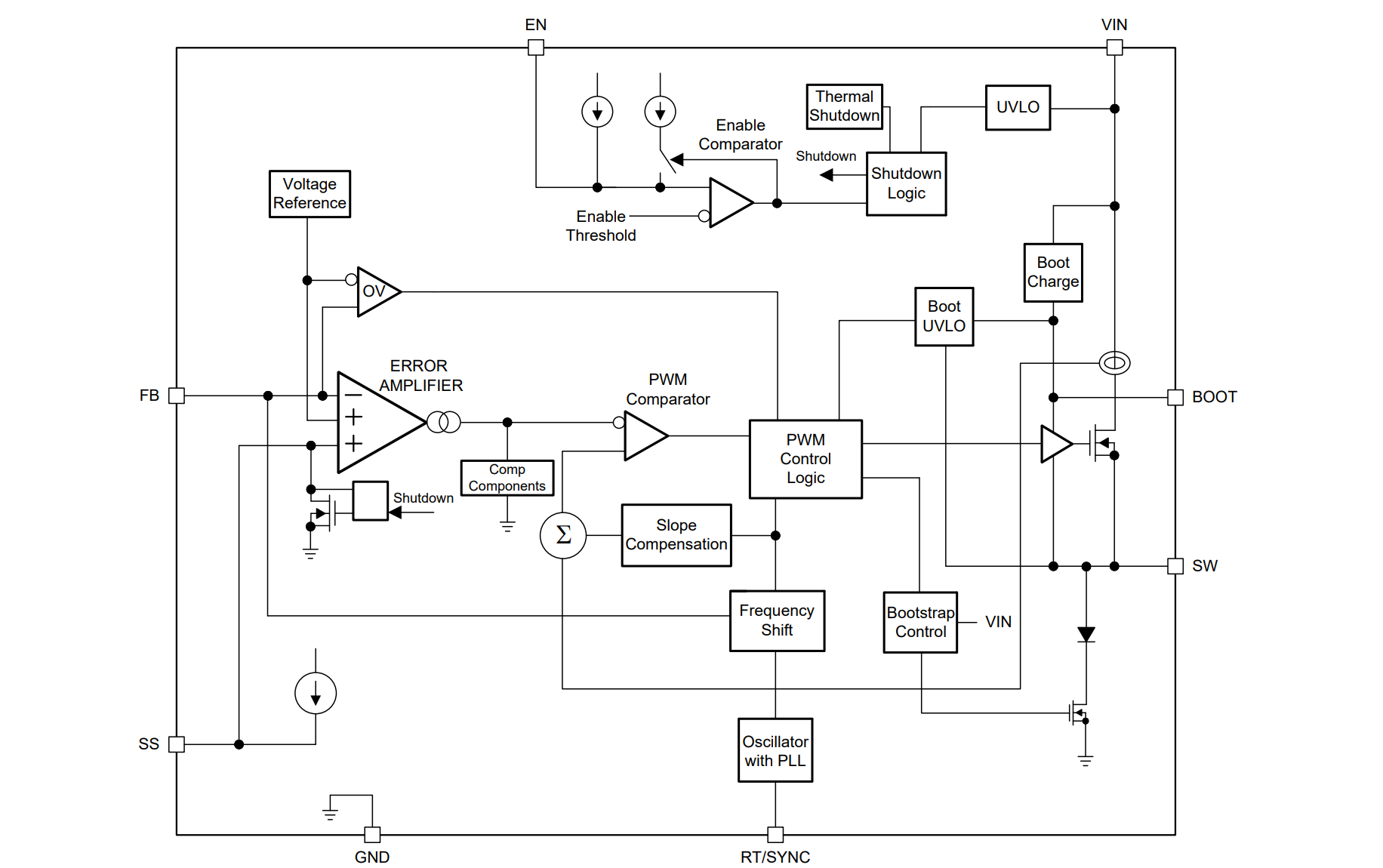
Pin Definitions
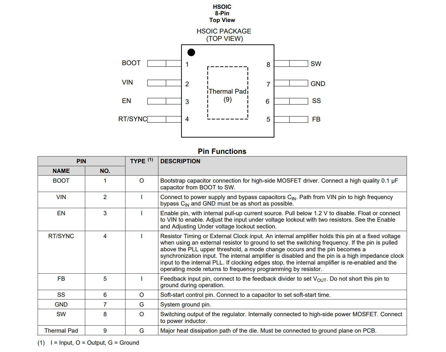
- BOOT: Bootstrap capacitor for the high-side MOSFET. Connect a 0.1uF capacitor between BOOT and SW.
- VIN: Power input, connected to this pin after coupling capacitor \(C_{IN}\).
- EN: Enable switch with internal pull-up. Pulling this pin below 1.2V will disable the output. Floating or connecting it to \(V_{IN}\) will enable the output. Refer to the following section for undervoltage lockout adjustment.
- RT/SYNC: Resistor-timed or external clock input. When using an external resistor to ground to set the switching frequency, the internal amplifier keeps this pin at a fixed voltage. If the pin is pulled above the PLL upper threshold, a mode change occurs and the pin becomes a synchronous input. The internal amplifier is disabled, and the pin becomes a high-impedance clock input for the internal PLL. If the clock edge stops, the internal amplifier is re-enabled, and the operation mode returns to frequency programming through the resistor.?
- FB: Feedback input pin, feedback is input through a resistor divider from \(V_{OUT}\), should not be directly connected to ground.
- SS: Soft-start control pin, connect a capacitor to set the soft-start time.
- SW: Regulated switch output, internally connected to the high-side MOSFET. Connect the power inductor to this pin.
Feature Description
Voltage Regulation Principle
The output voltage of LMR14050 is adjusted by opening the high-side N-MOS and controlling the conduction time. During the conduction of the high-side N-MOS, the voltage at the SW pin swings to approximately \(V_{IN}\), and the inductor current iL increases with a linear slope of (\(V_{IN}\) - \(V_{OUT}\)) / L. When the high-side N-MOS is turned off, the inductor current discharges with a slope of \(V_{OUT}\) / L through the freewheeling diode. The control parameters of the regulator are determined by the duty cycle D = \(t_{ON}\) / \(T_{SW}\), where \(t_{ON}\) is the high-side switch conduction time and \(T_{SW}\) is the switching period. The regulator control loop adjusts the duty cycle D to maintain a constant output voltage. In an ideal buck converter, losses are neglected, and D is directly proportional to the output voltage and inversely proportional to the input voltage: D = \(V_{OUT}\) / \(V_{IN}\).
The relationship between the SW voltage and the inductor current in Continuous Conduction Mode (CCM) is shown below:

Sleep Mode
The sleep mode is activated under light load conditions to improve efficiency and reduce gate drive losses by minimizing switch transitions. The sleep mode is triggered if the peak output current is below 300mA.
BOOT Bootstrap Circuit Design
LMR14050 integrates an internal bootstrap voltage converter. By connecting a bootstrap capacitor to the BOOT and SW pins, a voltage sufficient to drive the gate of the high-side MOSFET can be provided. The recommended value for the BOOT capacitor is 0.1uF (X7R or X5R ceramic capacitor with a minimum voltage rating of 16V).
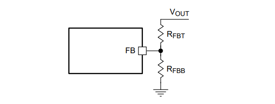
Output Voltage Regulation
LMR14050 provides an internal reference voltage of 0.75V. The output voltage is divided from \(V_{OUT}\) through a resistor divider and fed into the FB pin for internal comparison and regulation. It is recommended to use resistors with a deviation of 1% or lower and a temperature coefficient of 100 ppm or lower for the voltage divider. The low-side resistor \(R_{FBB}\) (recommended value is 10-100kΩ) is chosen based on the desired voltage division current, and the high-side resistor \(R_{FBT}\) is calculated using the formula. Choosing a larger resistor value helps improve light load efficiency, but if it is too large, the regulator will be more susceptible to noise and voltage errors from the FB input current.
EN Enable and Undervoltage Lockout Adjustment
LMR14050 turns on the output when \(V_{IN}\) is above 3.7V and EN is above the 1.2V threshold. The regulator shuts down when \(V_{IN}\) drops below 3.52V or EN falls below 1.2V. EN has an internal pull-up current source (1uA) to ensure normal output when the EN pin is floating.
The external pull-up and pull-down resistors for EN can be adjusted to set the startup and shutdown voltage thresholds:
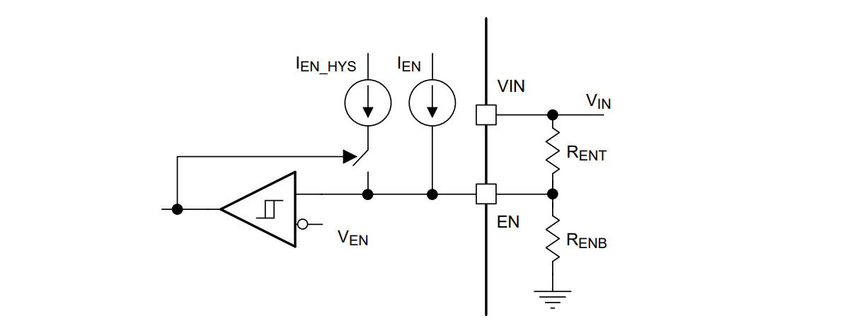
\(R_{ENT}\) and \(R_{ENB}\) are calculated using the following formulas:
where \(V_{START}\) is the desired startup voltage threshold, \(V_{STOP}\) is the desired undervoltage shutdown voltage threshold, and \(I_{HYS}\) is the hysteresis current from EN when the voltage exceeds 1.2V (typical value is 3.6uA).
External Soft-Start
Soft-start is used to mitigate the inrush current to the regulator and load during power-up. It can be configured by connecting an external capacitor \(C_{SS}\) between the SS and GND pins. There is an internal current source \(I_{SS}\) (typical value is 3uA) that charges the capacitor and generates a ramp from 0V to \(V_{REF}\). The soft-start time can be configured using the following formula:
\(t_{SS}(ms)=\frac{C_{SS}(nF)*V_{REF}(V)}{I_{SS}(uA)}\)
The soft-start is reset when the regulator is disabled or internally shut down.
Switching Frequency and Synchronization (RT/SYNC)
The switching frequency of LMR14050 can be programmed by connecting a resistor \(R_T\) between RT/SYNC and GND. The RT/SYNC pin should not be left floating or connected to ground. The resistance value can be determined using the following formula or chart:

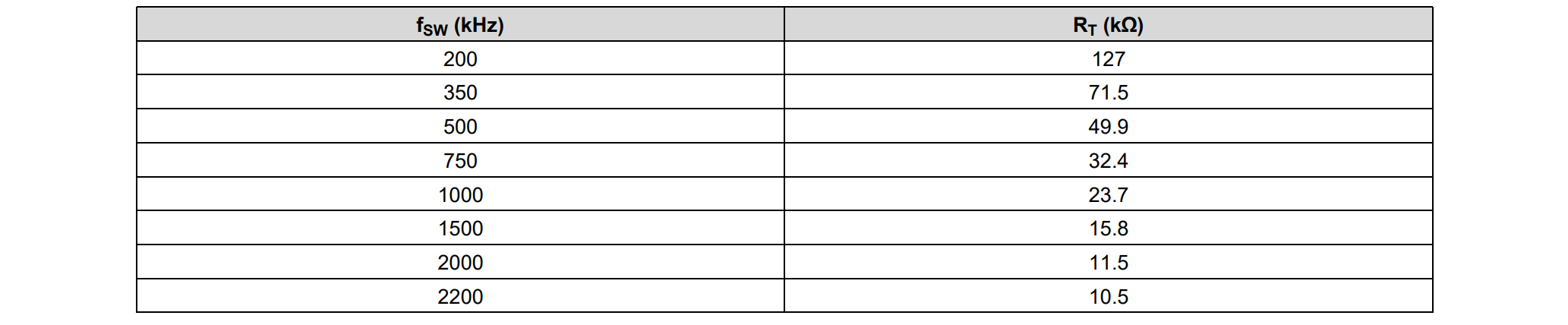
The switching action of LMR14050 can also be synchronized with an external clock input signal (250kHz-2.3MHz):
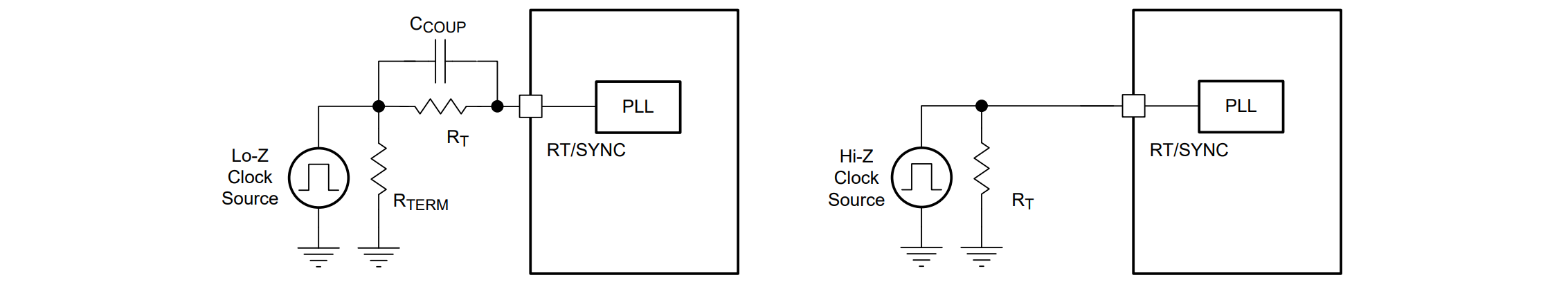
The internal oscillator will be synchronized with the falling edge of the external clock. The recommended high level of the external clock should not be lower than 1.7V, the low level should not be higher than 0.5V, and the minimum pulse width should not be less than 30ns. If a low impedance signal source is connected, the frequency-setting resistor \(R_T\) needs to be connected in parallel with an AC coupling resistor \(C_{COUP}\) (which can be a 10pF ceramic capacitor) and terminated with a terminal resistor \(R_{TERM}\) (e.g., 50Ω) to achieve better impedance matching.
Overcurrent and Short Circuit Protection
LMR14050 provides cycle-by-cycle current limiting for the high-side MOSFET to prevent overcurrent conditions. The peak current of the high-side switch is compared with the output of the error amplifier (EA) minus the slope compensation in each switching cycle. The peak current of the high-side switch is limited by a constant clamp maximum peak current threshold. Therefore, the peak current limitation of the high-side switch is not affected by the slope compensation and remains constant throughout the entire duty cycle range.
Overvoltage Protection
LMR14050 has built-in output overvoltage protection (OVP) circuitry to minimize voltage overshoot. When the FB voltage reaches the rising OVP threshold (109% of VREF), the high-side MOSFET is turned off; when it drops below the falling OVP threshold (107% of VREF), the high-side MOSFET resumes normal operation.
Thermal Shutdown Protection
LMR14050 has internal thermal shutdown protection. When the junction temperature exceeds 170℃, the thermal shutdown is activated and the high-side MOSFET stops switching. The internal soft restart will occur only when the chip temperature drops below 158℃.
Reference Design
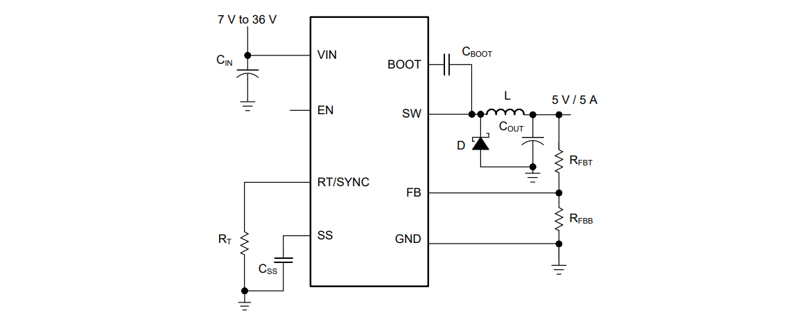
Design parameters:
- Input voltage \(V_{IN}\): 7-36V, typical value is 12V
- Output voltage \(V_{OUT}\): 5V
- Maximum output current \(I_{O\_MAX}\): 5A
- Transient response (0.5-5A): 5%
- Output voltage ripple: 50mV
- Input voltage ripple: 400mV
- Switching frequency \(f_{SW}\): 300kHz
- Soft-start time: 5ms
Output Voltage Setting
According to the formula above, if we need an output voltage of 5V, we can choose \(R_{FBT}\) as 100kΩ and \(R_{FBB}\) as 17.4kΩ (approximated to 17.65kΩ, balanced for tuning losses).
If we need an output voltage of 12V, we can choose \(R_{FBT}\) as 100kΩ and \(R_{FBB}\) as 6.34kΩ (approximated to 6.666kΩ, balanced for tuning losses).
Switching Frequency Setting
We choose a switching frequency of 300kHz, and according to the formula above, \(R_T\) should be selected as 84.5kΩ (approximated to 83.9kΩ).
Output Inductor Selection
In DC-DC converters, the most critical parameters of an inductor are its inductance value, saturation current, and RMS current. The selection of the inductance value is based on the desired peak-to-peak ripple current \(Δi_L\). Since the ripple current increases with the input voltage, the maximum input voltage is always used to calculate the minimum inductance value \(L_{MIN}\). The minimum value of the output inductor can be calculated using the following formulas:
Among them, \(K_{IND}\) is the coefficient that represents the ripple current of the inductor relative to the maximum output current, and a reasonable value should be 20%-40%. During instantaneous short-circuit or overcurrent operation events, the RMS and peak inductor currents may be high. The rated value of the inductor current should be higher than the current limit.
Generally speaking, the lower the inductance value, the better, because it usually brings faster transient response, smaller DCR, and smaller size. However, too low inductance value may result in larger inductor current ripple, which may mistakenly trigger overcurrent protection during full load. Due to slightly higher RMS current, it also generates more conduction losses. Larger inductor current ripple also means larger output voltage ripple. For peak current mode control, it is not recommended to have too small inductor current ripple, and larger peak current ripple can improve the signal-to-noise ratio of the comparator.
In the reference design, the value of \(K_{IND}\) is set to 0.4, so the minimum inductance value is calculated to be 7.17uH, and the closest value is 8.2uH. An 8.2 μH ferrite inductor with a 7A RMS current and a 10A saturation current can be selected.
Output Capacitor Selection
The selection of output capacitor \(C_{OUT}\) directly affects the steady-state output voltage ripple, loop stability, and voltage overshoot and undershoot during load current transients. The output ripple consists of two parts. One is caused by the inductor current ripple through the equivalent series resistance (ESR) of the output capacitor:
The other is caused by the inductor current ripple charging and discharging the output capacitor:
These two voltage ripples are not in phase, so the actual peak-to-peak ripple will be smaller than the sum of the two.
If the system requires strict voltage regulation (large current step and fast slew rate), the output capacitor will be constrained by transient performance specifications. When there is a rapid increase in the load, the output capacitor can provide the required charge before the inductor current rises to the appropriate level. The control loop of the regulator usually requires at least three clock cycles to respond to the output voltage drop. The output capacitor must be large enough to provide the current difference of three clock cycles to keep the output voltage within the specified range.
When the load suddenly decreases significantly, the output capacitor absorbs the energy stored in the inductor. The clamping diode cannot conduct current, so the energy in the inductor will cause the output voltage to overshoot. The formula for calculating the minimum output capacitance required for a specific undershoot is:
\(C_{OUT}>\frac{3*(I_{OH}-I_{OL})}{f_{SW}*V_{US}}\)
The formula for calculating the minimum capacitance required to keep the voltage overshoot within a specified range is:
\(C_{OUT}>\frac{I_{OH}^2-I_{OL}^2}{(V_{OUT}+V_{OS})^2-V_{OUT}^2}*L\)
where,
- \(K_{IND}\) is the ripple ratio of inductor ripple current (\(Δi_L/I_{OUT}\))
- \(I_{OL}\) is the low-level output current during load transient
- \(I_{OH}\) is the high-level output current during load transient
- \(V_{US}\) is the target undershoot of the output voltage
- \(V_{OS}\) is the target overshoot of the output voltage
In the reference design, the target output ripple is 50mV. Assuming \(ΔV_{OUT\_ESR}=ΔV_{OUT\_C}=50mV\), \(K_{IND}\) is set to 0.4, \(ESR\) is not greater than 25mΩ, and \(C_{OUT}\) is not less than 16.7 μF, the overshoot and undershoot range of the reference design is \(V_{US}=V_{OS}=5%*V_{OUT}=250mV\). Therefore, \(C_{OUT}\) can be calculated to be not less than 180uF and 79.2uF respectively, so the stricter standard of 180uF is chosen, that is, 4 47uF (16V, X7R ceramic capacitors with ESR of 5mΩ) are connected in parallel.
Schottky Diode Selection
The rated breakdown voltage of the diode is best 25% higher than the maximum input voltage. For optimal reliability, the rated current of the diode should be equal to the maximum output current of the regulator. When the input voltage is much higher than the output voltage, the average current of the diode will be lower, and a diode with a lower rated average current, approximately \((1-D) * I_{OUT}\), can be used. However, the peak current rating should be higher than the maximum load current. Generally, a starting point of 6-7A is chosen.
Input Capacitor Selection
LMR14050 requires high-frequency input decoupling capacitors and large-capacity input capacitors. The typical recommended value for high-frequency decoupling capacitors is 4.7-10 μF (X5R/X7R, ceramic capacitors with a voltage rating of more than twice the maximum input voltage). In the reference design, two 2.2 μF X7R ceramic capacitors with a rated voltage of 100 V are used. The high-frequency filtering capacitor needs to be placed close to the regulator.
Large capacitance capacitors provide damping for voltage spikes, with reference values of 47uF or 100uF electrolytic capacitors.
BOOT Capacitor Selection
LMR14050 requires a BOOT capacitor, as mentioned earlier, the reference value for the BOOT capacitor is 0.1uF (X7R or X5R ceramic capacitor, with a minimum voltage rating of 16V).
Soft-Start Capacitor Selection
According to the previous formula, if the soft-start time is set to 5ms, the recommended soft-start capacitor value is 22nF (close to the calculated value of 20nF).
Layout Recommendations
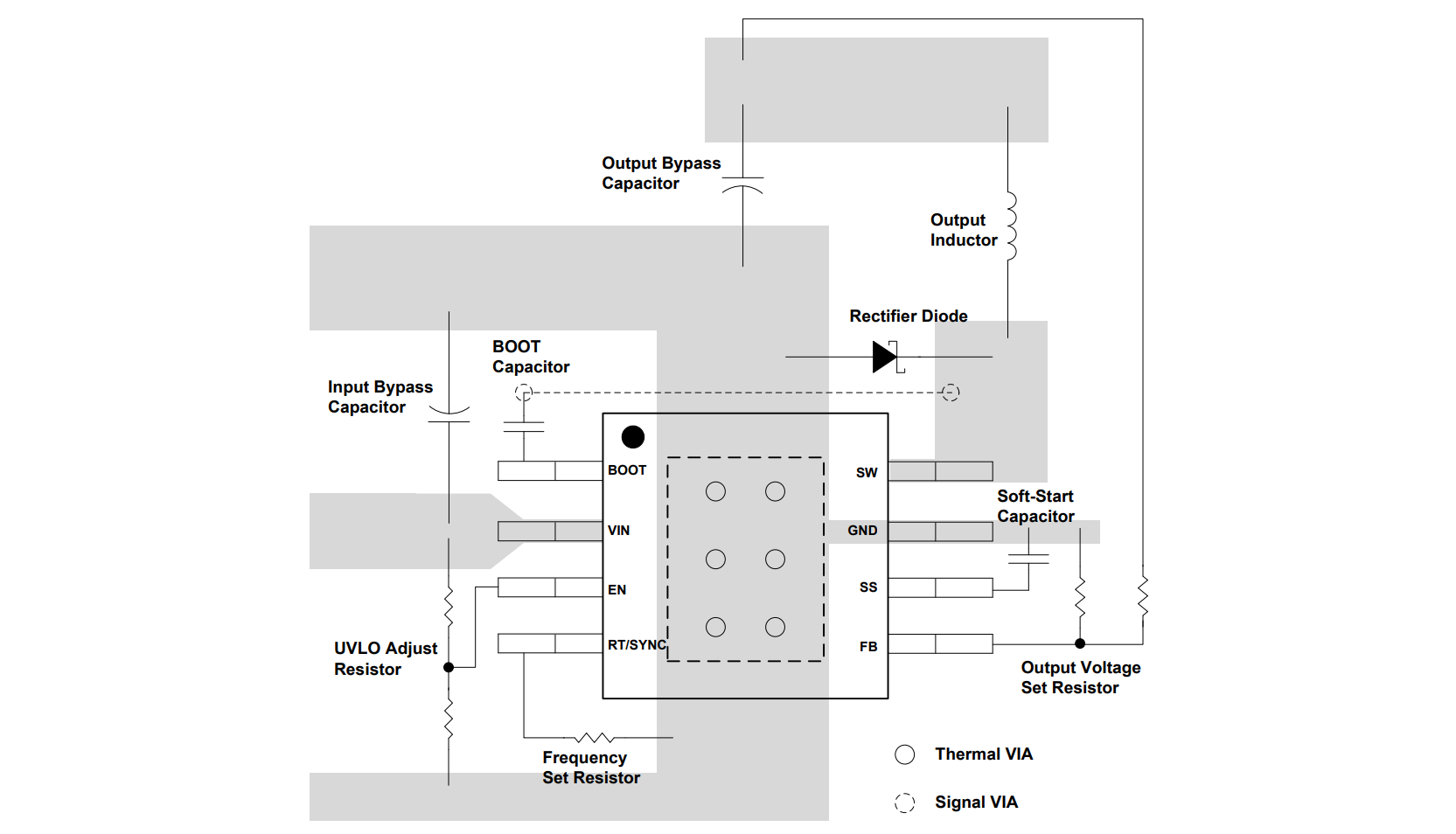
Layout recommendations for reducing EMI:
- The feedback network, resistors \(R_{FBT}\) and \(R_{FBB}\) should be placed as close as possible to the FB pin. The sampling path of \(V_{OUT}\) should be far away from noise-generating paths, preferably on the other side of the shielding layer.
- Input decoupling capacitors should be placed as close as possible to \(V_{IN}\) and GND.
- Inductors should be placed close to the SW pin to reduce magnetic and electrostatic noise.
- The output capacitor \(C_{OUT}\) should be placed close to the node of the inductor and diode, with short traces to reduce conducted and radiated noise and improve efficiency.
- The grounding connections of the diode, \(C_{IN}\), and \(C_{OUT}\) should be kept as small as possible and connected at only one point (preferably at the ground connection of \(C_{OUT}\)) to minimize conducted noise in the system ground layer.
Actual Testing
With a 24V input and a 5V/5A full load output, the actual output is 4.95V/5.00A, with a ripple of 15mV and a temperature of 110℃.
References and Acknowledgments
Original: https://wiki-power.com/ This post is protected by CC BY-NC-SA 4.0 agreement, should be reproduced with attribution.
This post is translated using ChatGPT, please feedback if any omissions.