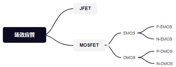
Basic Components - Field Effect Transistor
A field effect transistor (FET) is a device that controls current with voltage. Among them, the MOSFET we commonly use is a field effect transistor composed of metal, oxide, and semiconductor. The following text focuses on the introduction of the enhancement mode N-channel MOSFET.
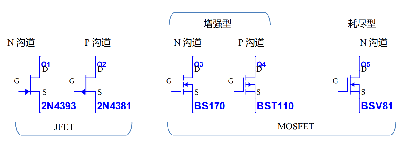
The pins of the field effect transistor correspond to those of the bipolar transistor: the gate (G) corresponds to the base (b), the drain (D) corresponds to the collector (c), and the source (S) corresponds to the emitter (e). The arrow indicates the direction of electron movement.
In normal operation, there is no current at the gate of the field effect transistor. Therefore, the drain current must be equal to the source current. The core of the field effect transistor is to control the drain current with the voltage between the gate and source (GS). Therefore, it is also called a voltage-controlled component.
Pin Definitions of MOSFET
The MOSFET has three pins (G, S, D) defined as follows:
- G: gate
- S: source
- D: drain
The power supply of the N-channel is generally connected to D and the output is connected to S. The power supply of the P-channel is generally connected to S and the output is connected to D. The connection methods for enhancement mode and depletion mode are basically the same.
The source and drain of the MOSFET can be interchanged. They are both N-type regions formed in the P-type backgate. In most cases, these two regions are the same, and even if they are interchanged, it will not affect the performance.
Parasitic Diode
Due to the manufacturing process, the MOSFET has a parasitic diode, also known as a body diode.
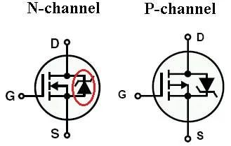
When the conduction condition of the MOSFET is met, the drain and source of the MOSFET will conduct, and at this time, the body diode is in the cutoff state. Because the conduction resistance of the MOSFET is very small, it is not enough to make the parasitic diode conduct.
Conduction Conditions of MOSFET
The MOSFET is voltage-controlled, and whether it conducts is determined by the voltage difference between the gate and source (GS).
For N-MOS, it conducts when \(V_g-V_s>V_{gs(th)}\).
For P-MOS, it conducts when \(V_s-V_g>V_{gs(th)}\).
Characteristics of Enhancement Mode MOSFET
The structure of the enhancement mode MOSFET is to create two N-type channels on a P-type silicon substrate, and use aluminum to lead out two electrodes as the source (S) and drain (D) (at this time, D/S can be interchanged). Then, a thin layer of SiO2 insulation layer is covered on the surface of the semiconductor, and an aluminum electrode is installed on the insulation layer between the drain and source, serving as the gate (G), and an electrode is also led out on the substrate. Because the substrate is already connected to the source during the manufacturing process, D/S cannot be interchanged at this time.
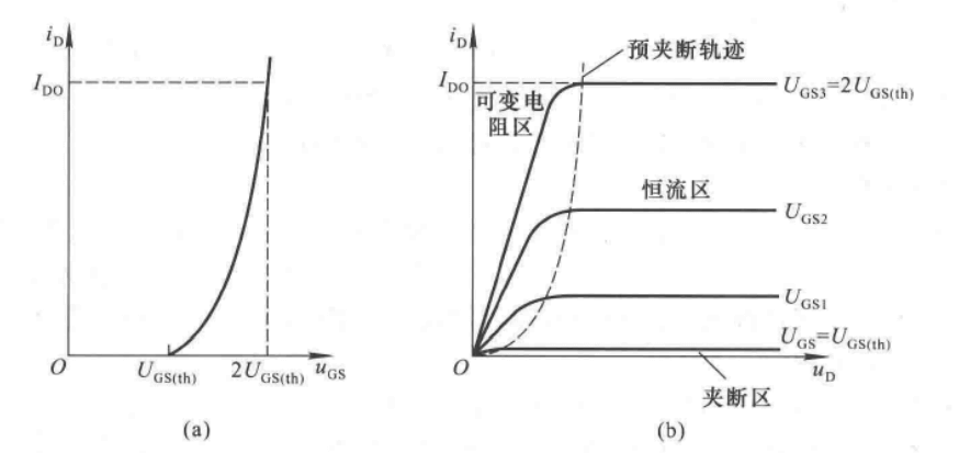
The graph shows the voltage-current characteristics of the enhancement mode MOSFET. The left graph is the transfer characteristics, and the right graph is the output characteristics. They share the same vertical axis.
Key elements of the voltage-current characteristics:
- Threshold voltage \(U_{GS_(th)}\): From the graph, it can be seen that \(U_{GS_(th)} = 1V\). When \(U_{GS} < U_{GS_(th)}\), regardless of the magnitude of \(U_{DS}\), the current \(i_D\) is always 0. Only when \(U_{GS} > U_{GS_(th)}\), the MOSFET is considered to be turned on.
- Ohmic region equation: \(i_D = K(u_{GS}-U_{GS_(th)})^2\), where K affects the growth rate of the transfer characteristics curve (unit: \(A/V^2\)).
- Boundary between variable resistance region and constant current region: As \(U_{GS}\) increases, the boundary voltage \(U_{DS_{dv}}\) also increases, and it satisfies \(U_{DS_{dv}}=U_{GS} - U_{GS_(th)}\).
Operating States of MOSFET
MOSFET is different from a bipolar transistor. Because some models have parallel diodes inside the package, the D and S terminals cannot be reversed, and the N-channel must flow from D to S, and the P-channel must flow from S to D. The operating states can be determined using the following table:
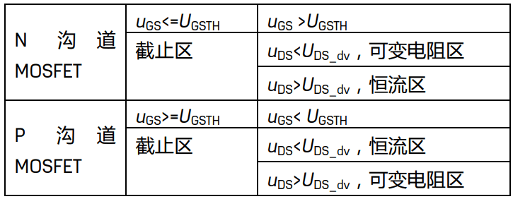
Several operating regions:
- Cutoff Region: When \(U_{GS}\) is less than the threshold voltage \(U_{GS_(th)}\), the MOSFET does not conduct.
- Variable Resistance Region: \(U_{DS}\) is small, and \(I_D\) increases with the increase of \(U_{DS}\).
- Saturation Region: \(U_{DS}\) changes, and \(I_D\) changes very little.
- Breakdown Region: When \(U_{DS}\) reaches a certain value, the MOSFET breaks down, and \(I_D\) suddenly increases. Without a current-limiting resistor, it will be damaged.
- Over-dissipation Region: High power dissipation, requires enhanced heat dissipation, pay attention to the maximum power.
Main Parameters of MOSFET
DC Parameters:
- Threshold Voltage \(U_{GS_(th)}\): Parameter for enhancement-mode MOSFET. It refers to the minimum value of \(\left| u_{GS} \right|\) required to make \(i_D > 0\) when \(U_{DS}\) is constant.
- Off Voltage \(U_{GS_(off)}\): Parameter for depletion-mode MOSFET. Similar to \(U_{GS_(th)}\), it represents \(u_{GS}\) when \(i_D\) is a specified small current and \(U_{DS}\) is constant.
- DC Input Resistance \(U_{GS_(DC)}\): The ratio of gate-source voltage to gate current. Generally, \(U_{GS_(DC)}\) of MOSFET is greater than \(10^9 \Omega\).
Key Selection Parameters:
- Breakdown Voltage V_BRDSS
- Should have a margin for temperature variation.
- On-state Resistance R_DS(on)
- Positive temperature coefficient of on-state resistance, suitable for parallel operation.
- The smaller the on-state resistance, the smaller the conduction loss.
- The smaller the on-state resistance, the larger the Qg, and the slower the corresponding switching speed.
- It brings larger switching losses, and needs to be considered in a trade-off manner for high-frequency operation.
- Maximum Junction Temperature
- Must never exceed the maximum junction temperature.
- Can only be calculated by measuring the case temperature and using thermal resistance.
- Dynamic Capacitance and Qg
- Not fixed values, depend on operating conditions.
- When used as a switch, fast turn-on is desired, requiring a driver chip to provide a large instantaneous current.
- When used as a soft-start MOSFET, slow turn-on is required to effectively suppress surge current.
N-MOS:
- The gate needs a higher voltage drive than the source.
- Better performance.
- More choices.
- Lower cost.
P-MOS:
- The gate needs a lower voltage drive than the source.
- No need for higher voltage drive, simple drive.
Comparison between Transistors and MOSFETs
| Transistor | MOSFET | |
|---|---|---|
| Type | Current Control | Voltage Control |
| Input Impedance | Low | High |
| Noise | High | Low |
| Response Speed | Fast | Slow |
Feedback
Definition: Returning a portion or all of the output signal (voltage / current) of an amplification circuit back to the input and superimposing it with the input signal.
Negative Feedback: The returned signal weakens the input signal. Positive Feedback: The returned signal enhances the input signal.
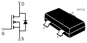
Common Packages for MOSFETs
SOT Package
SOT (Small Out-Line Transistor) package is generally used for low-power MOSFETs.
SOT-23 Package:
SOT-89 Package:
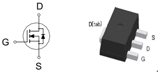
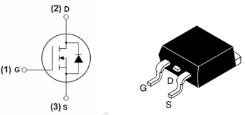
TO Package
TO (Transistor Out-line) is an earlier packaging specification, originally mostly in through-hole packages (such as TO-92, TO-220, TO-252), and later evolved into surface-mount packages. TO-252 and TO-263 are typical examples, where TO-252 is also known as D-PAK, and TO-263 is also known as D2PAK.
The MOS transistors packaged in D-PAK have three electrodes, among which the drain electrode (D) pin is cut off and not used. Instead, the backside heat sink plate is used as the drain electrode, allowing for greater current output and better heat dissipation.
TO-252 package:
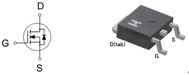
TO-263 package:
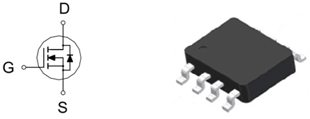
SOP package
SOP (Small Out-Line Package), also known as SO, SOL, or DFP. It usually comes in variations such as SOP-8, SOP-16, SOP-20, SOP-28, etc. (the number indicates the number of pins). Most MOS transistors in SOP package adopt the SOP-8 specification.
SOP-8 package:
References and Acknowledgements
- Knowledge and arrangement of surface mount MOS transistors
- All you need to know about MOS transistors
Original: https://wiki-power.com/ This post is protected by CC BY-NC-SA 4.0 agreement, should be reproduced with attribution.
This post is translated using ChatGPT, please feedback if any omissions.