Semiconductor Testing Basics - AC Parameter Testing
AC testing ensures that the time characteristics of the Device Under Test (DUT) meet its specification requirements.
Basic AC Parameters
Setup Time
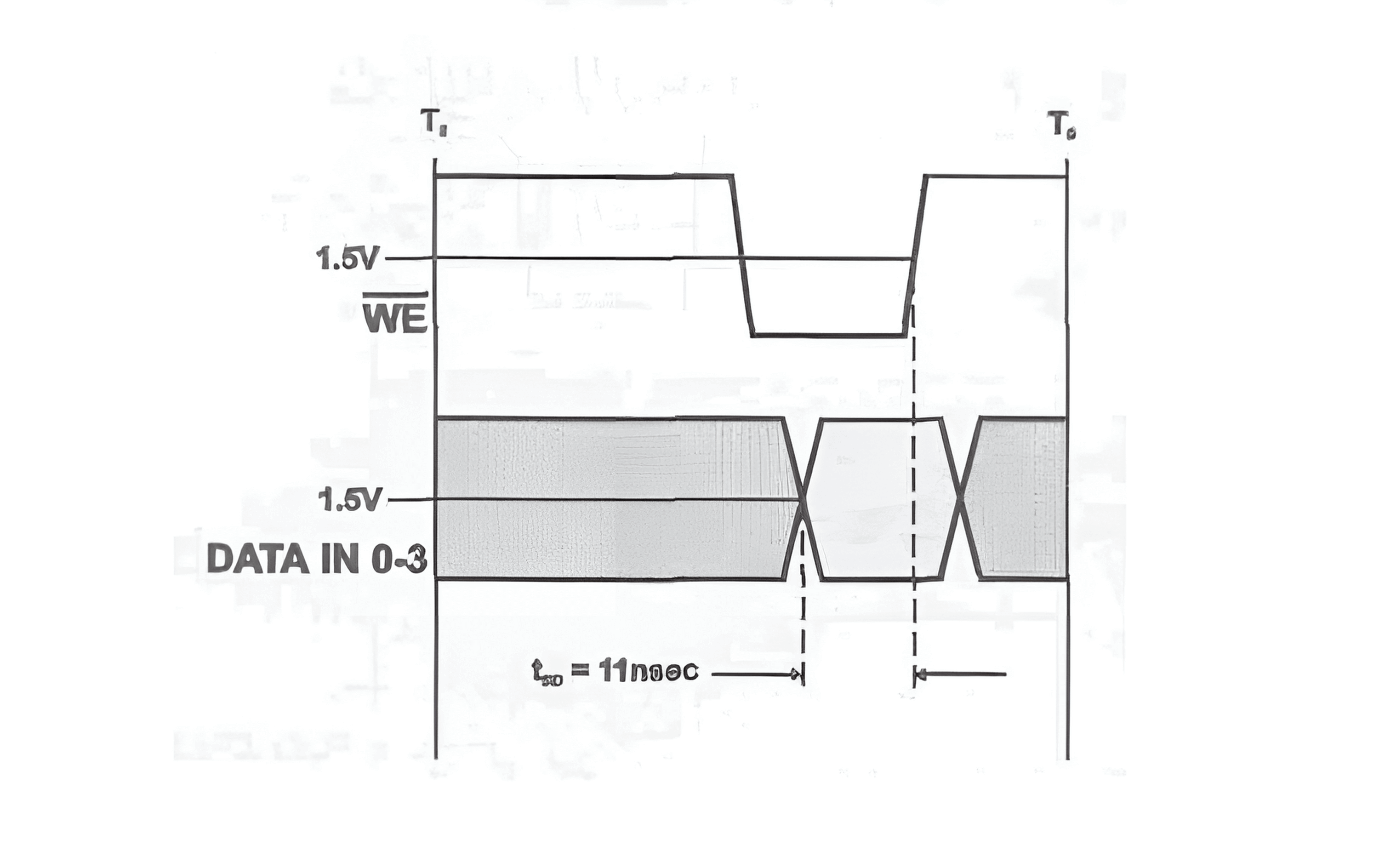
Setup time refers to the minimum time data (labeled as DATA IN in the diagram) must remain stable and unchanged before the reference signal (shown as WE in the figure) undergoes a change (reaching a midpoint of 1.5V). This stability is essential to ensure correct data reading. Data can change freely before the minimum setup time is reached, but if it remains stable too late, it may not be recognized, leading to errors. The specification in the datasheet is represented as follows:
| Parameter | Description | Min | Max | Unit |
|---|---|---|---|---|
| \(t_{SD}\) | Data Set-Up to Write End | 11 | ns |
Hold Time
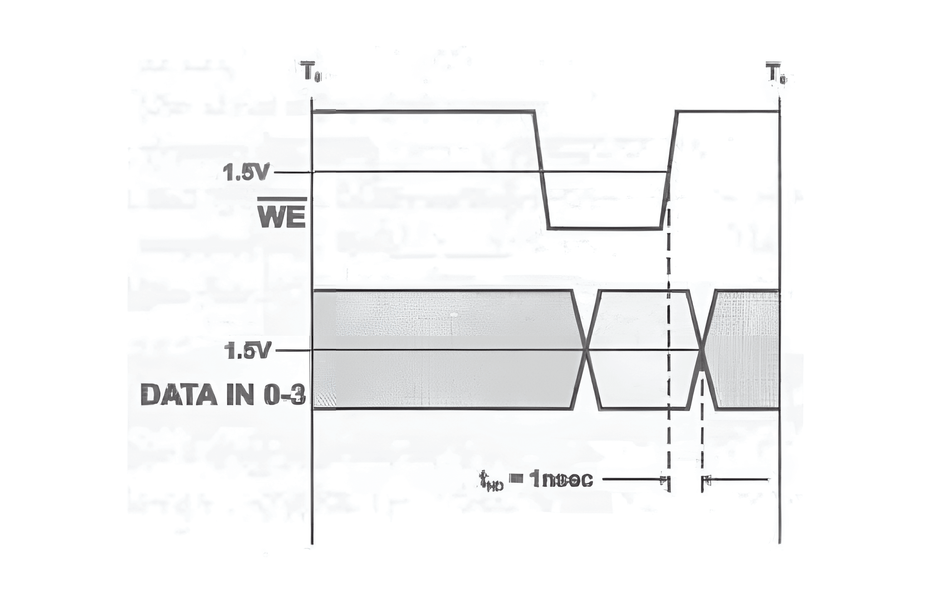
Hold time refers to the minimum duration that data (depicted as DATA IN in the diagram) must remain stable after the reference signal (depicted as WE in the figure) undergoes a change (reaching a certain voltage threshold). This duration ensures error-free data handling or maintaining a stable voltage level for a specific time before a clock signal triggers. If the hold time is too short, there is a probability that the data may not be correctly recognized. The specification in the datasheet is represented as follows:
| Parameter | Description | Min | Max | Unit |
|---|---|---|---|---|
| \(t_{HD}\) | Data Hold from Write End | 1 | ns |
Propagation Delay
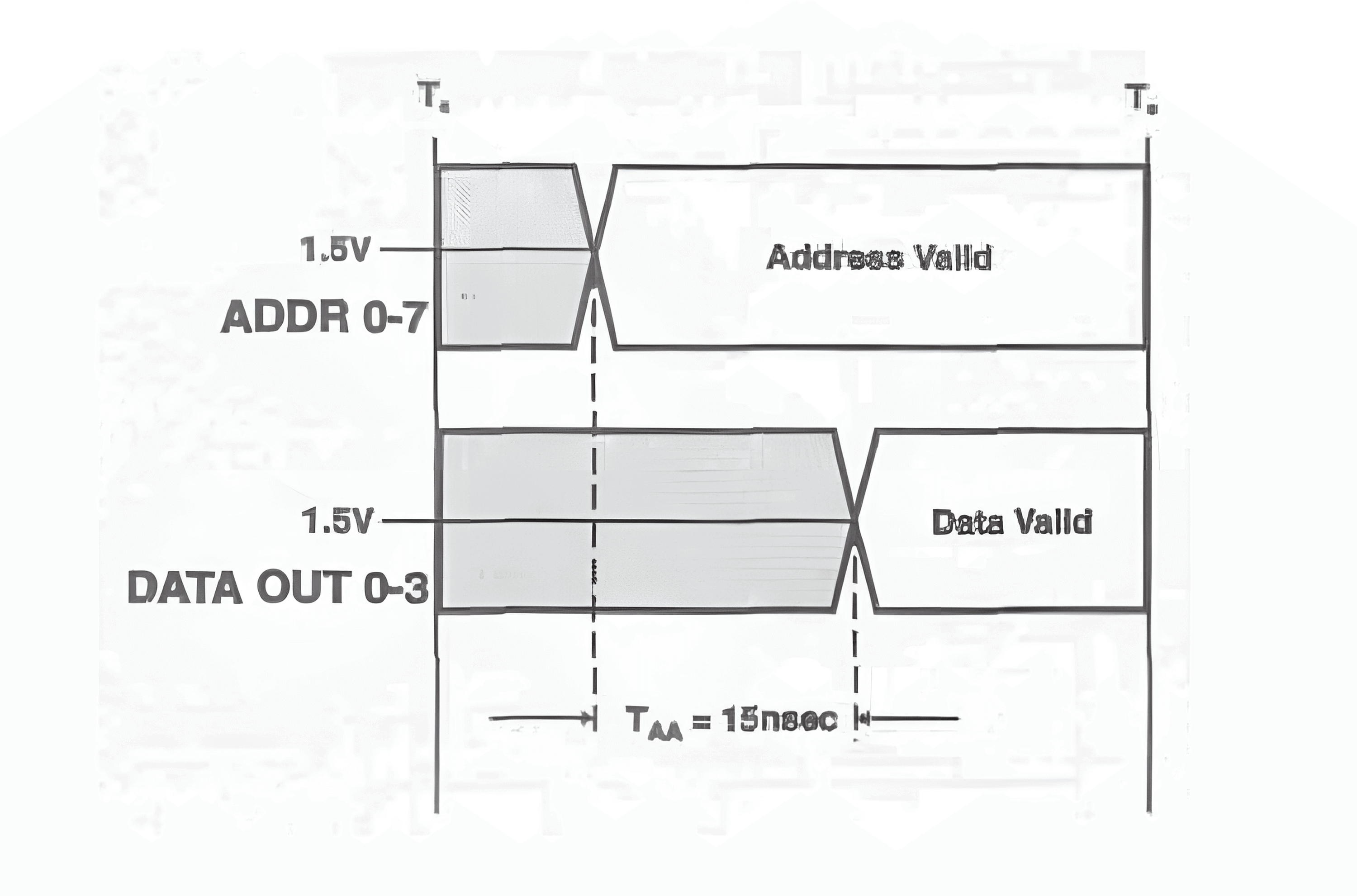
Propagation delay refers to the time interval between the transmission of one signal and the response of another related signal. Typically, it measures the time gap between a change in the input signal (labeled as ADDR in the diagram) and the corresponding output (labeled as DATA OUT) reaction, indicating the time required from the input side to the output side. It ensures that the output signal appears within a certain time after the input signal's occurrence. The specification in the datasheet is represented as follows:
| Parameter | Description | Min | Max | Unit |
|---|---|---|---|---|
| \(t_{AA}\) | Address to Data Valid | 15 | ns |
Minimum Pulse Widths
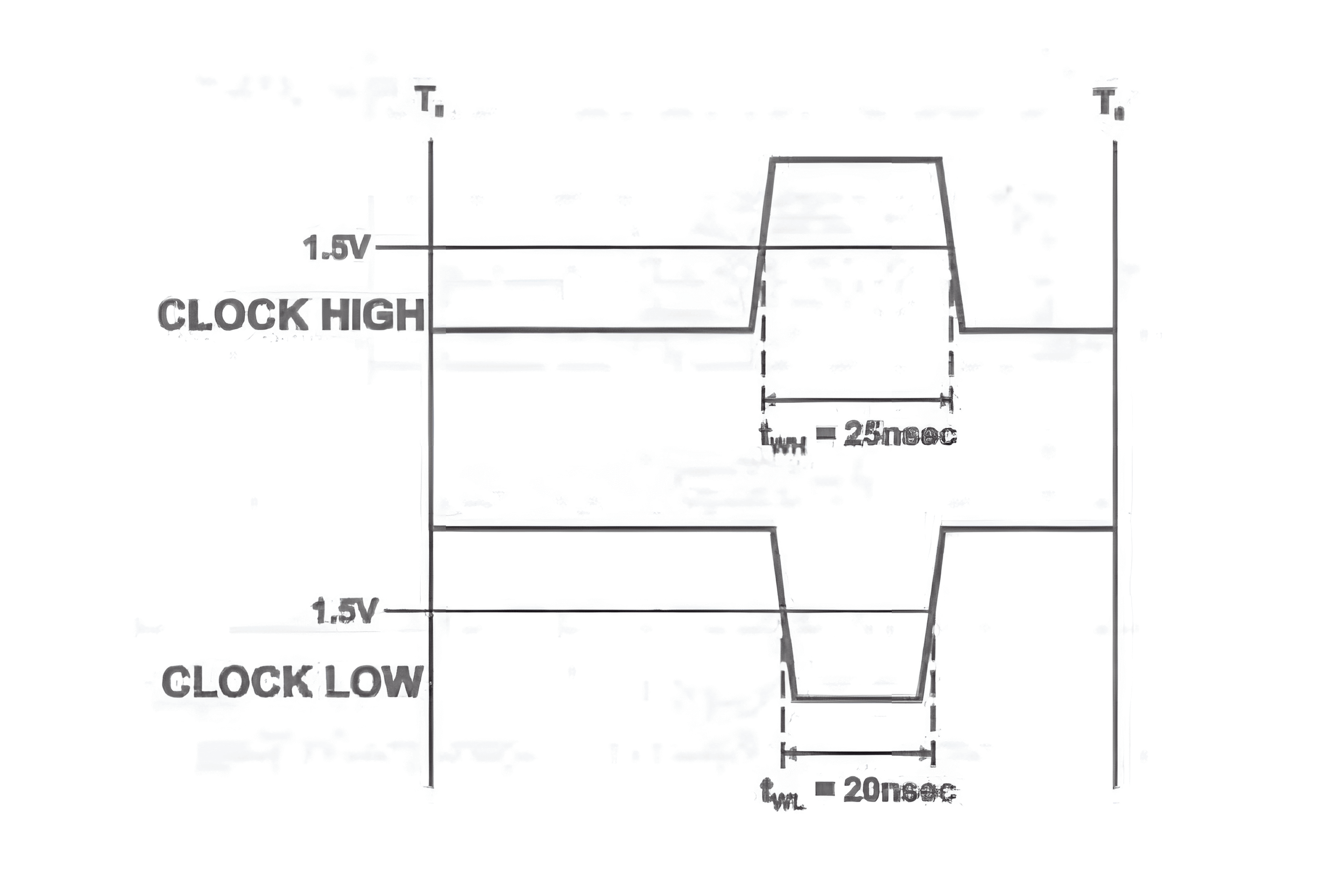
Minimum pulse widths typically include the minimum low pulse width and minimum high pulse width. These are used to ensure the minimum operable value for timing of pulses. The specification in the datasheet is represented as follows:
| Parameter | Description | Min | Max | Unit |
|---|---|---|---|---|
| \(t_{WL}\) | Minimum clock low time | 20 | ns | |
| \(t_{WH}\) | Minimum clock high time | 25 | ns |
Maximum Frequency
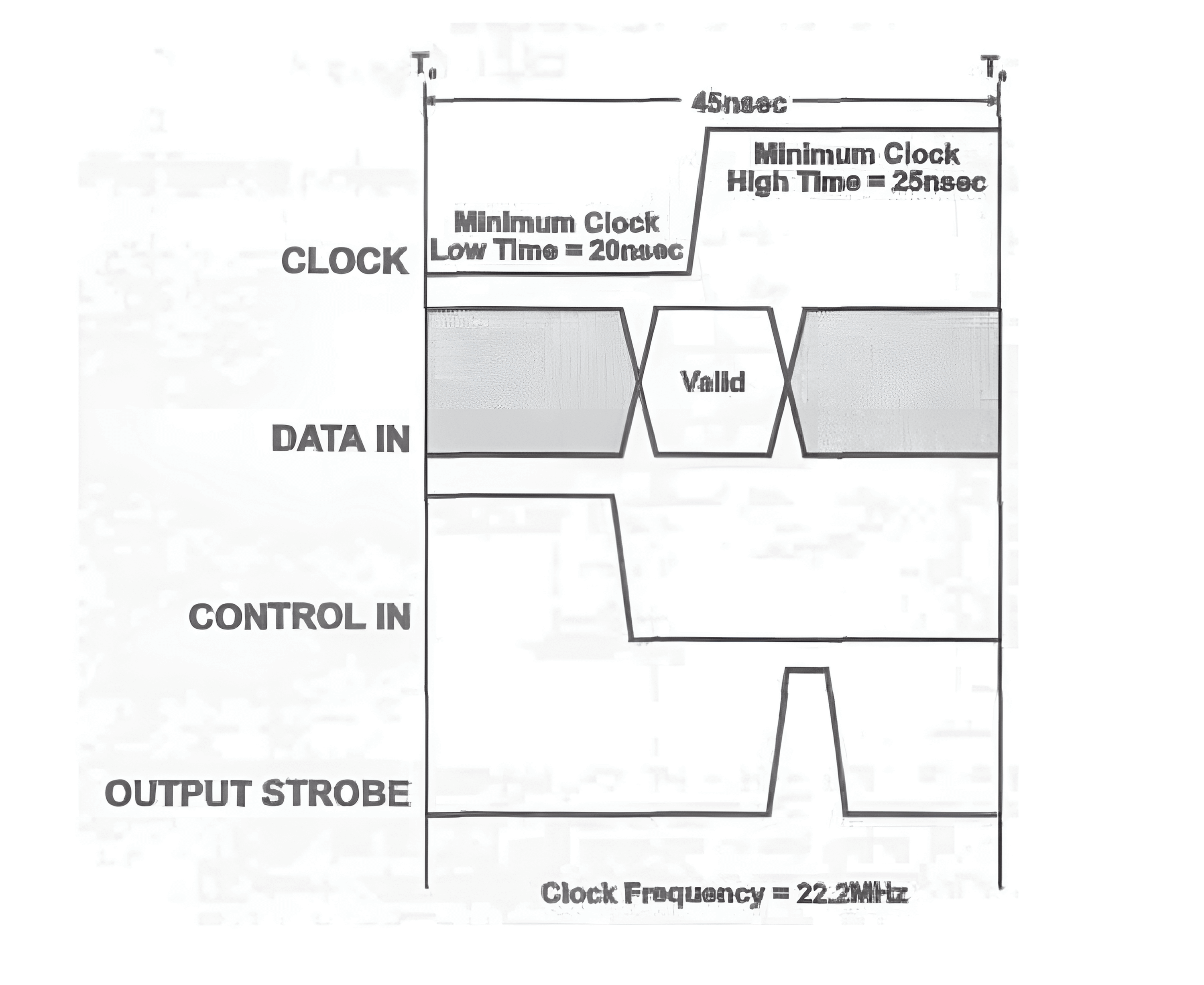
In plain terms, the maximum operating frequency refers to the highest speed at which a device can function. It's represented in the specifications as follows:
| Parameter | Description | Min | Max | Unit |
|---|---|---|---|---|
| \(f_{MAX}\) | Maximum clock frequency | 22.2 | MHz |
Output Enable Time
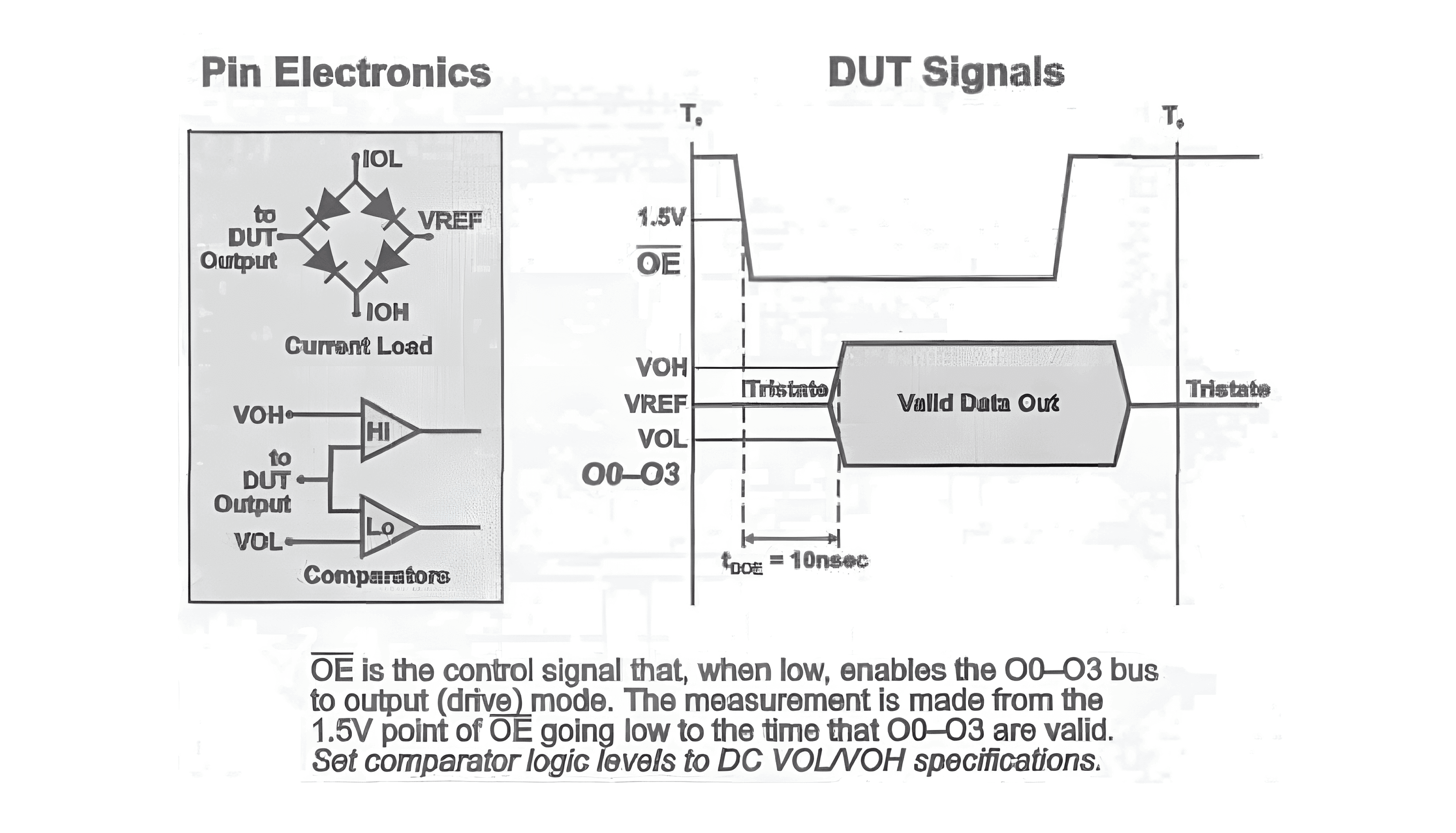
This refers to the time it takes for a pin to transition from a high-impedance state (disabled) to an active drive level (high or low). It ensures that the output buffer can change the pin state within the specified time. The representation in the specification is as follows:
| Parameter | Description | Min | Max | Unit |
|---|---|---|---|---|
| \(t_{DOE}\) | OE LOW to Data Valid | 10 | ns |
Output Disable Time
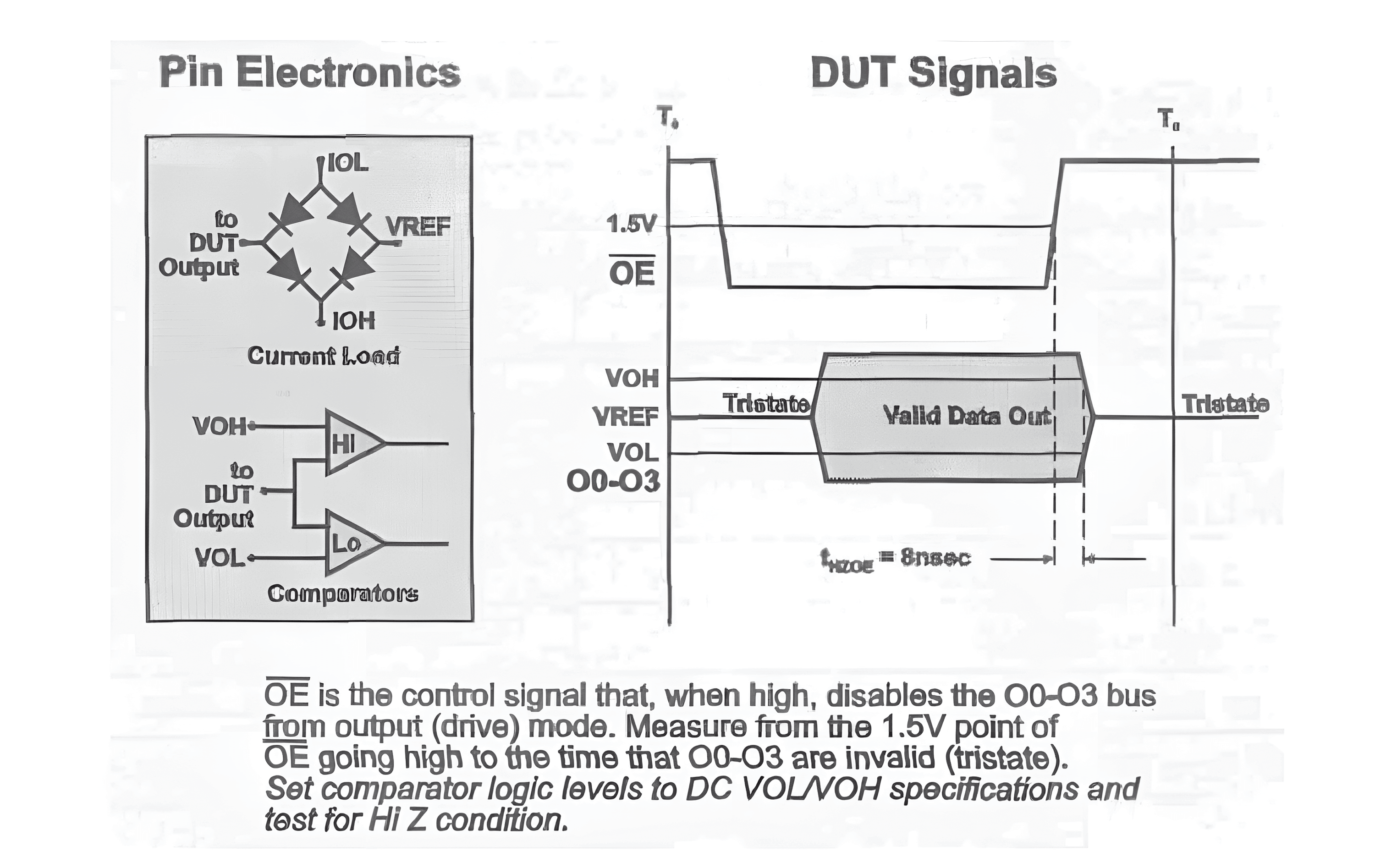
This refers to the time it takes for a pin to transition from an active drive level (high or low) to a high-impedance state (disabled). It ensures that the output buffer can change the pin state within the specified time. The representation in the specification is as follows:
| Parameter | Description | Min | Max | Unit |
|---|---|---|---|---|
| \(t_{HZOE}\) | OE High to Data Valid | 8 | ns |
Timing Parameters
Read Cycle Timing
An example of a read cycle for a 256 x 4 static RAM:
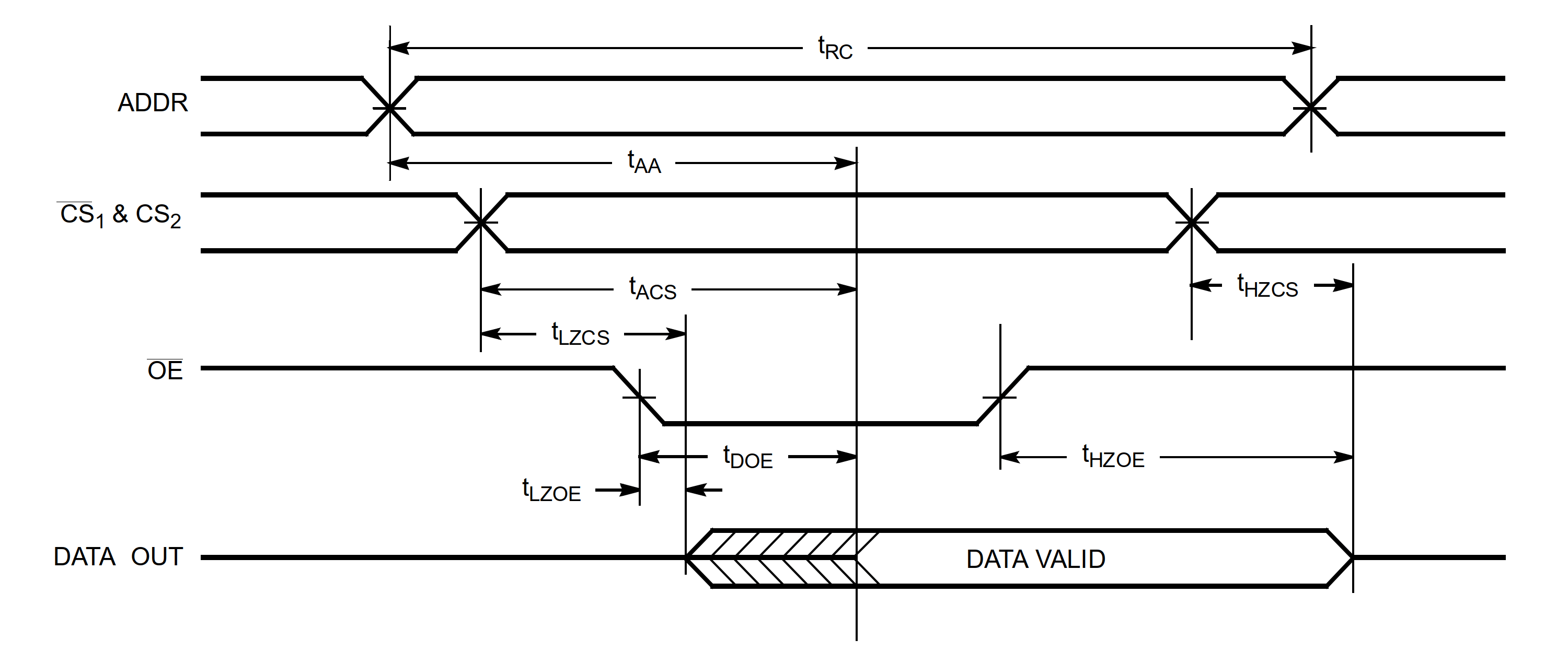
| Parameter | Description | Min | Max | Unit |
|---|---|---|---|---|
| \(t_{RC}\) | Read Cycle Time | 15 | ns | |
| \(t_{AA}\) | Address to Data Valid | 15 | ns | |
| \(t_{ACS}\) | Chip Select to Data Valid | 10 | ns | |
| \(t_{DOE}\) | OE LOW to Data Valid | 10 | ns | |
| \(t_{HZCS}\) | Chip Select to High Z | 8 | ns | |
| \(t_{HZOE}\) | OE HIGH to High Z | 8 | ns | |
| \(t_{LZCS}\) | Chip Select to Low Z | 2 | ns | |
| \(t_{LZOE}\) | OE LOW to Low | 2 | ns |
- First, the length of the write cycle is determined by the \(t_{RC}\) parameter.
- Identify which signal controls the read function. In the example in the diagram above, the data output of the RAM is controlled by the falling edge of OE.
Write Cycle Timing
An example of a write cycle for a 256 x 4 static RAM:
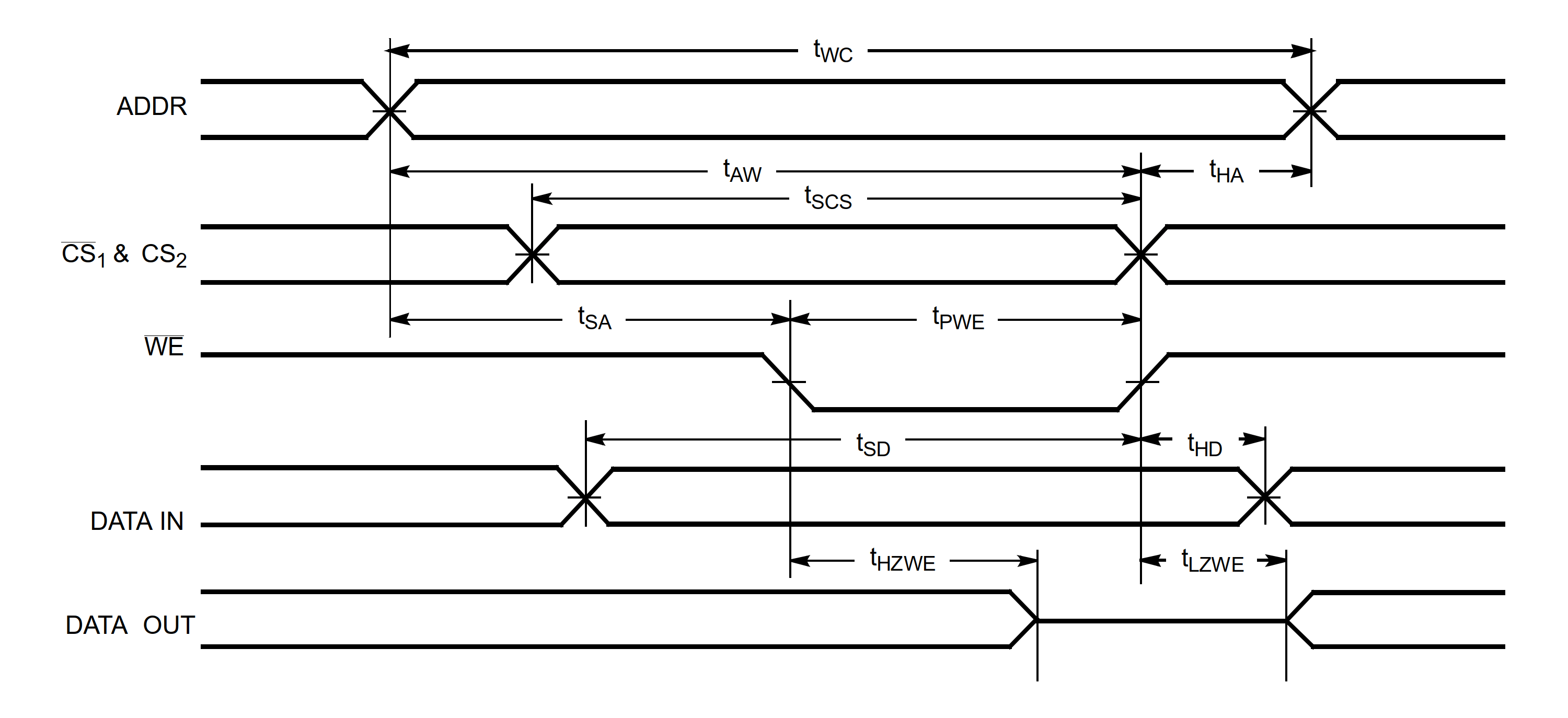
| Parameter | Description | Min | Max | Unit |
|---|---|---|---|---|
| \(t_{WC}\) | Write Cycle Time | 15 | ns | |
| \(t_{HZWE}\) | WE LOW to High Z | 8 | ns | |
| \(t_{LZWE}\) | WE HIGH to Low Z | 2 | ns | |
| \(t_{PWE}\) | WE Pulse Width | 11 | ns | |
| \(t_{SD}\) | Data Set-Up to Write End | 11 | ns | |
| \(t_{HD}\) | Data Hold from Write End | 1 | ns | |
| \(t_{SA}\) | Address Set-Up to Write Start | 2 | ns | |
| \(t_{HA}\) | Address Hold from Write End | 2 | ns | |
| \(t_{SCS}\) | CS LOW to Write End | 11 | ns | |
| \(t_{AW}\) | Address Set-Up to Write End | 13 | ns |
- First, the length of the write cycle is determined by the \(t_{WC}\) parameter.
- Identify which signal controls the write function. In the example in the diagram above, the data input to the RAM is controlled by the rising edge of WE.
References and Acknowledgments
- "The Fundamentals Of Digital Semiconductor Testing"
Original: https://wiki-power.com/ This post is protected by CC BY-NC-SA 4.0 agreement, should be reproduced with attribution.
This post is translated using ChatGPT, please feedback if any omissions.