Semiconductor Testing Basics - Basic Concepts
With the increasing integration of chips, manual testing is no longer sufficient to meet the demand, so automated test equipment (ATE) is used. Because chips are becoming more and more complex, ordinary bench testing cannot meet the requirements. ATE can detect the integrity of integrated circuit functions and is the final process in integrated circuit production and manufacturing, ensuring product quality. Chip testing is considered the most downstream component in the semiconductor industry chain. The devices under test (DUT) for testing are mainly divided into several categories: memory, digital circuits, analog circuits, and mixed-signal circuits.
ATE has many subsystems, including high and low level drive circuits, programmable current loads, voltage comparators for detecting output voltage, PMU connection circuits, high-speed current comparators, and high-speed switches.
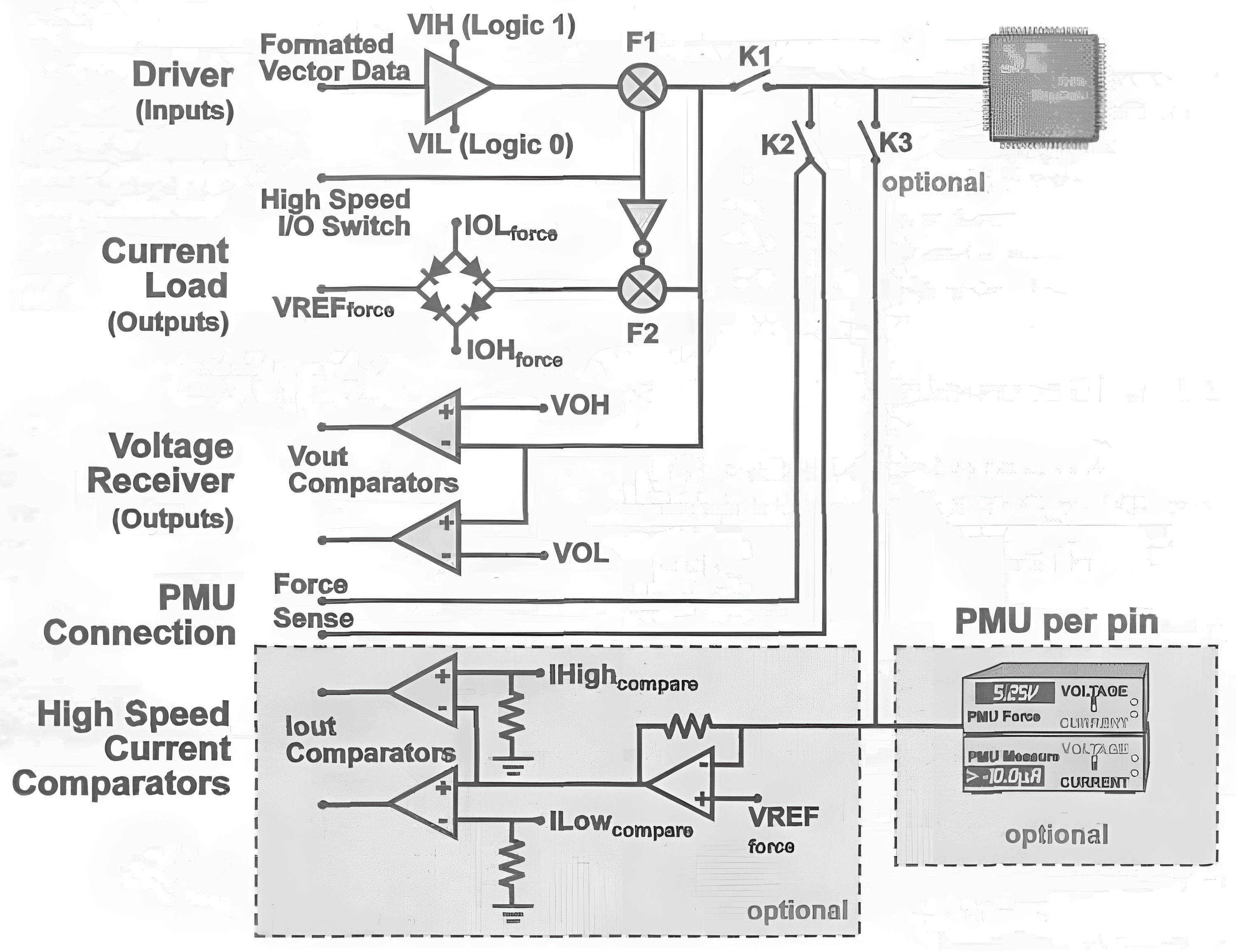
From the above figure, it can be seen that the testing system mainly consists of three parts: input, output, and dynamic load:
- Input section: Provides VIL/VIH voltage to the DUT.
- Output section: Compares the output voltage of the DUT with VOL/VOH.
- Dynamic load
- By loading IOL/IOH current, the output voltage is obtained and compared with VOL/VOH.
- Directly compares the output current with ILow/IHigh (usually only available on high-end machines).
The most basic testing involves measuring DC and AC parameters. The DC parameter measurement can be done using the Static method, which uses the PE card's driver and PMU to force V and measure I or force I and measure V. It can also be done using the Functional method, which uses current load and voltage comparators to run patterns for testing.
Signal Input and Output
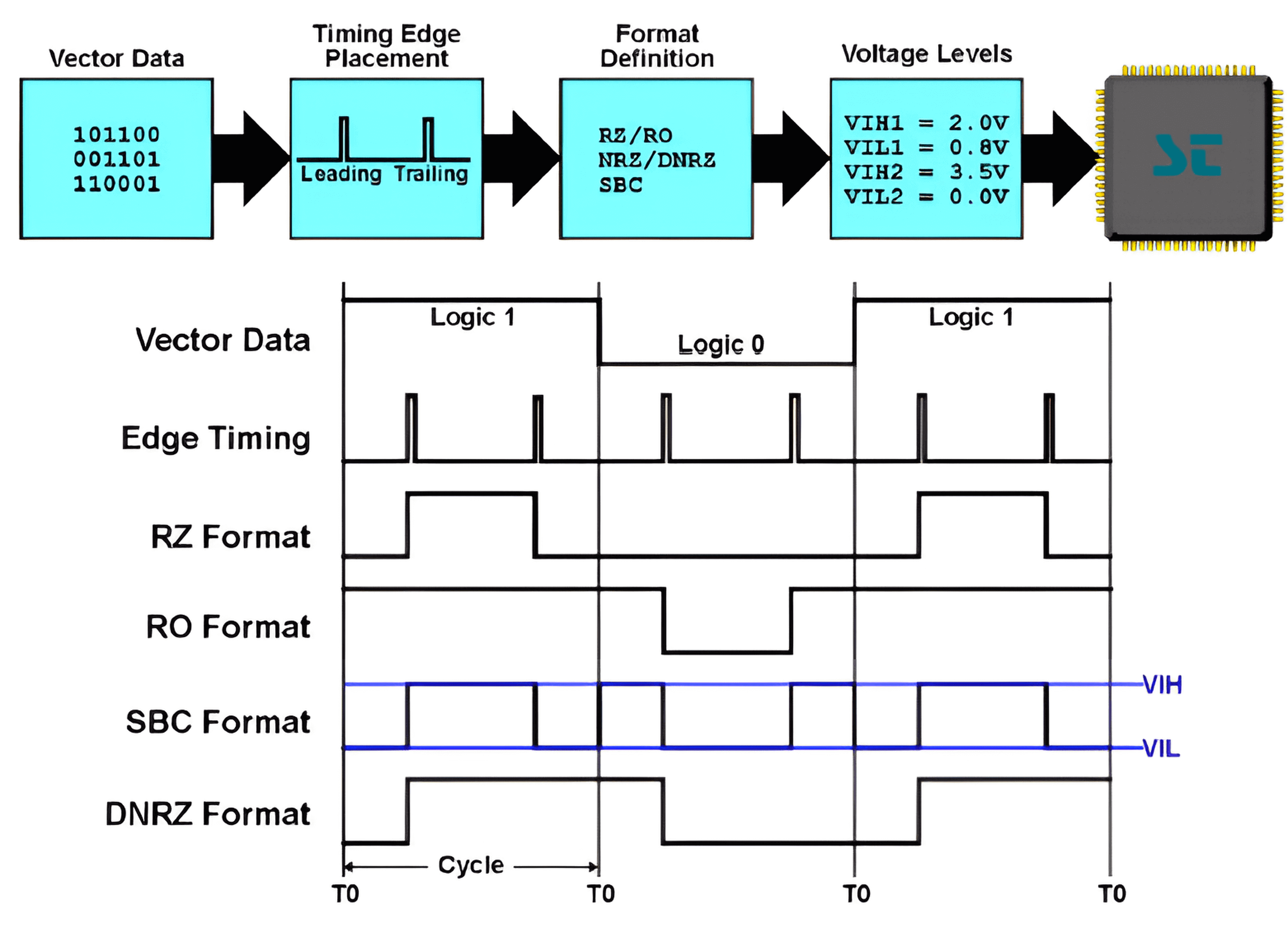
How signals are generated and input to the DUT:
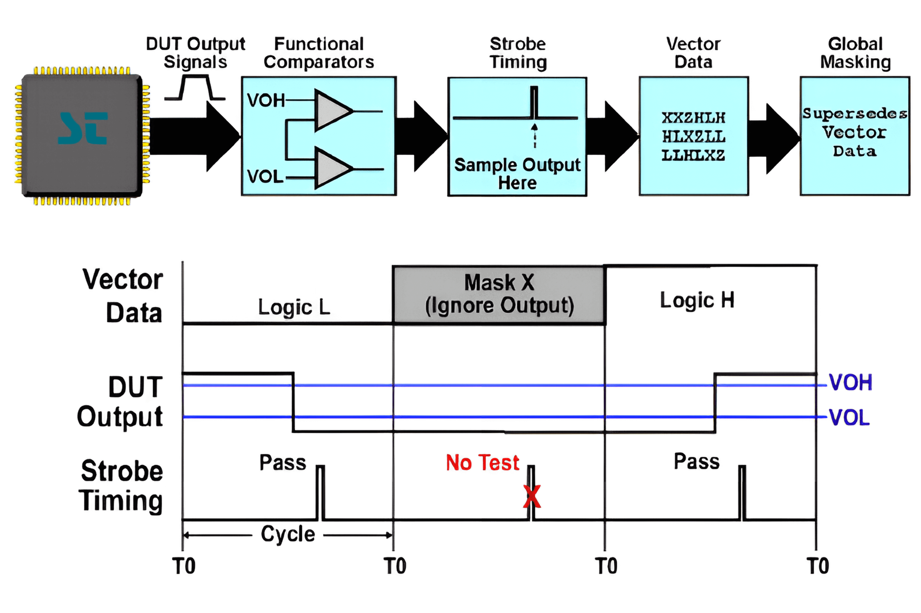
How signals are read from the DUT and tested:
Input Signal Formats
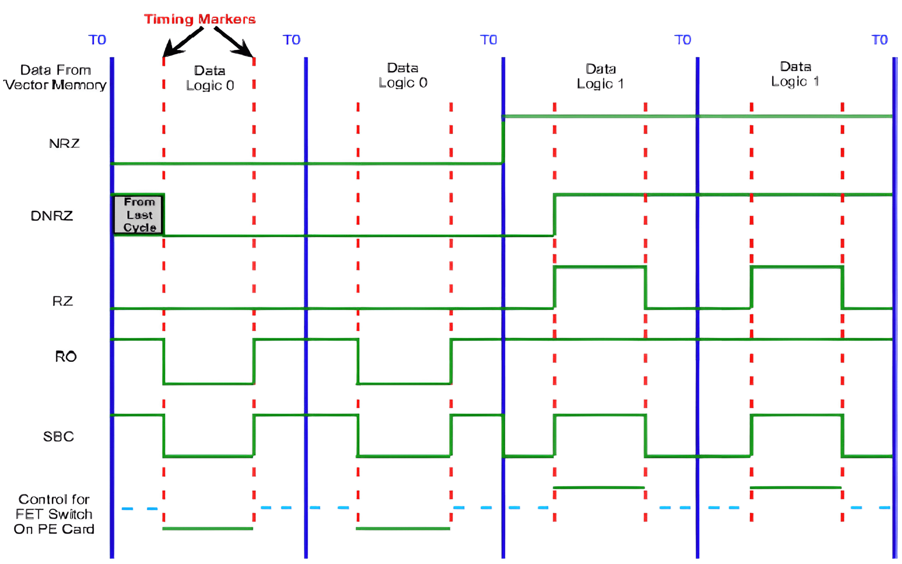
- RZ (Return to Zero): In this coding scheme, data bits are transmitted in binary within one cycle, and after the data bit pulse ends, a low level needs to be maintained. This coding scheme can simultaneously transmit clock and data signals, but the transmission efficiency is relatively low due to the occupation of some bandwidth by the zero level. The positions of the rising and falling edges can be controlled by Edge Timing.
- RO (Return to One): In this coding scheme, the opposite of RZ, a high level needs to be maintained. The positions of the rising and falling edges can be controlled by Edge Timing.
- NRZ (Non Return to Zero): The difference between NRZ and RZ is that NRZ does not need to return to zero, so one cycle can be used to transmit data, with a bandwidth utilization rate of 100%. If low-speed asynchronous data is transmitted, a clock line may not be required, but the communication baud rate needs to be agreed upon (such as UART); for high-speed synchronous data transmission, a separate clock line is required. NRZ is not controlled by Edge Timing.
- DNRZ (Delayed Non Return to Zero): DNRZ is an NRZ waveform with time delay. The delay time is controlled by Edge Timing.
- SBC (Surrounded By Complement): SBC is a combination of RZ and RO. It can have up to 3 edges within one cycle. At T0, the data is inverted, and after a certain delay, it appears as the preset value, and then it is inverted again after a certain time. SBC is mostly used for establishing/maintaining signal control.
- ZD (Impedance Drive): Impedance drive is used to control pin opening or closing (high impedance state).
Clock signals usually use RZ/RO formats, signals with rising edge validity (such as chip select CS or read READ) usually use RZ format, and signals with falling edge validity (such as output enable OE) usually use RO format. Data signals with setup and hold time requirements often use SBC format. Other input signals can use NRZ or DNRZ formats.
Output Signal Formats
High and Low Level Output
Translate into English:
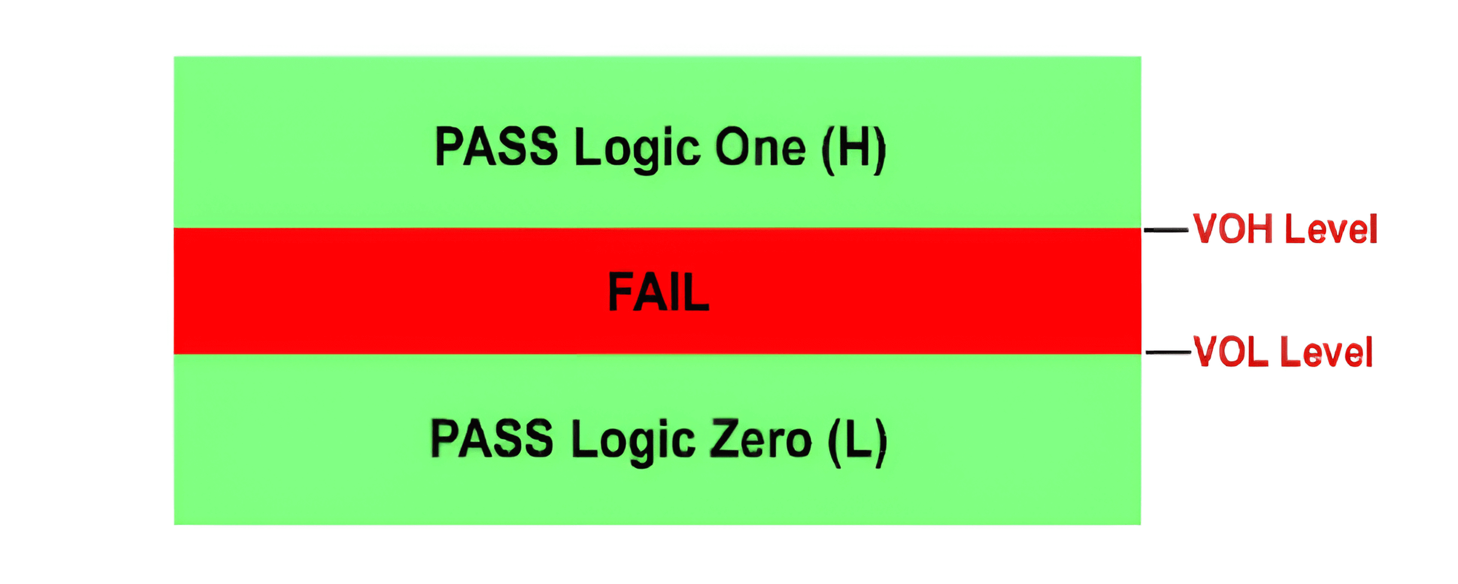
When the pin outputs a high or low logic level, the high level must be higher than VOH, and the low level must be lower than VOL.
High-impedance output
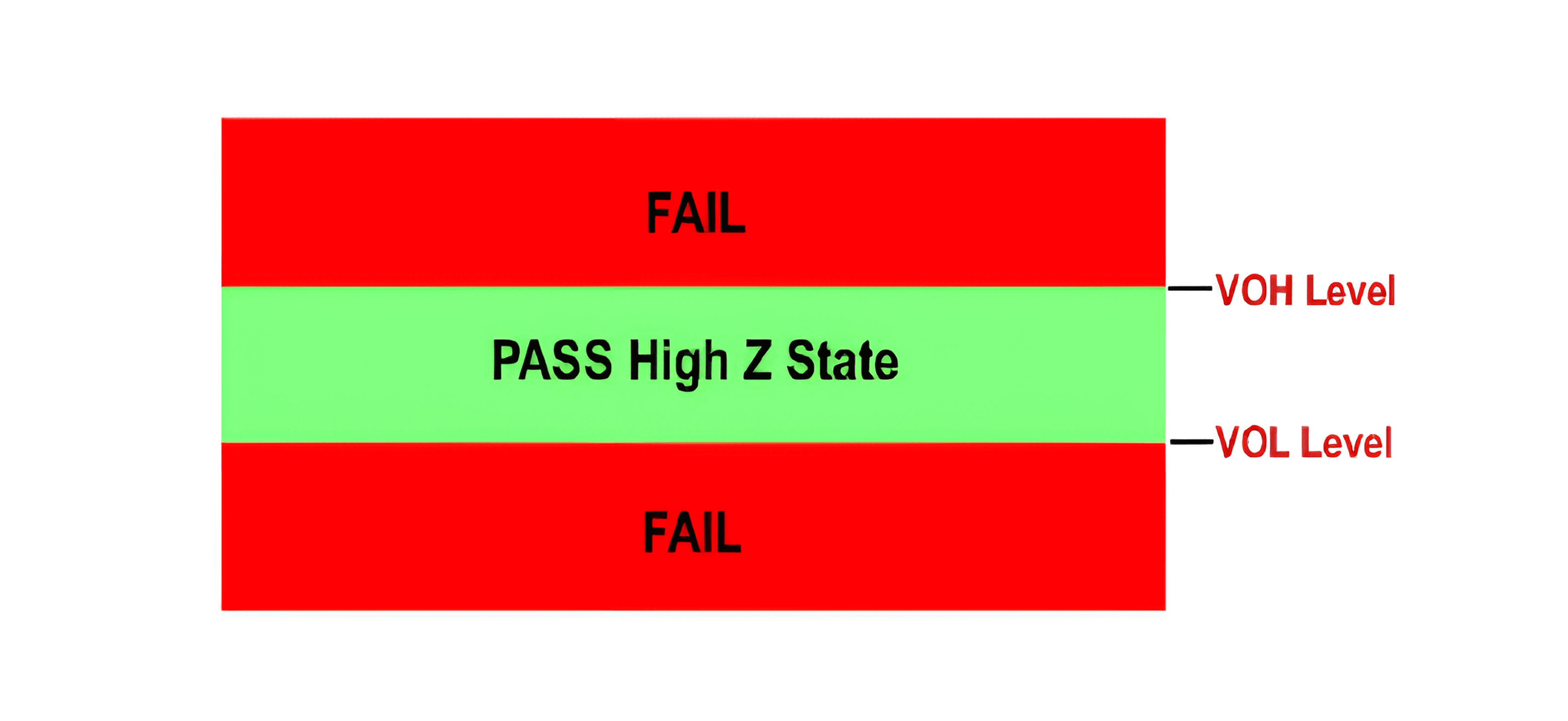
The DUT pin is pulled to a voltage between VOL and VOH by an external load and cannot output voltage or current.
Load current output
Some DUT pins can output load current. If the test system has a programmable current load, it can be tested directly. Otherwise, an external resistor may be required for testing. Load current output needs to output the specified IOL/IOH current when VOL/VOH meets the standard.
Explanation of Common Terms
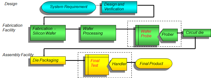
Wafer, Die, and Package
The process of chip design and manufacturing:
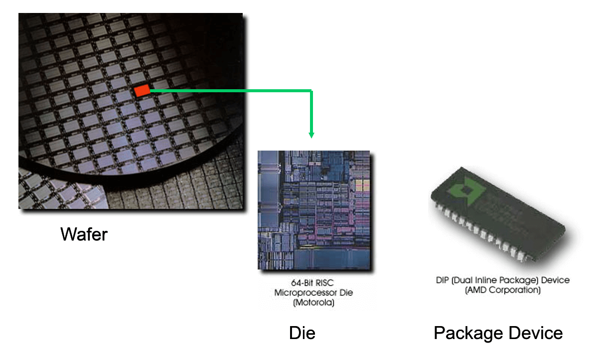
The relationship between the wafer, die (plural: dice), and packaged chip (package device) is as follows:
Wafer with testing and ink marking:
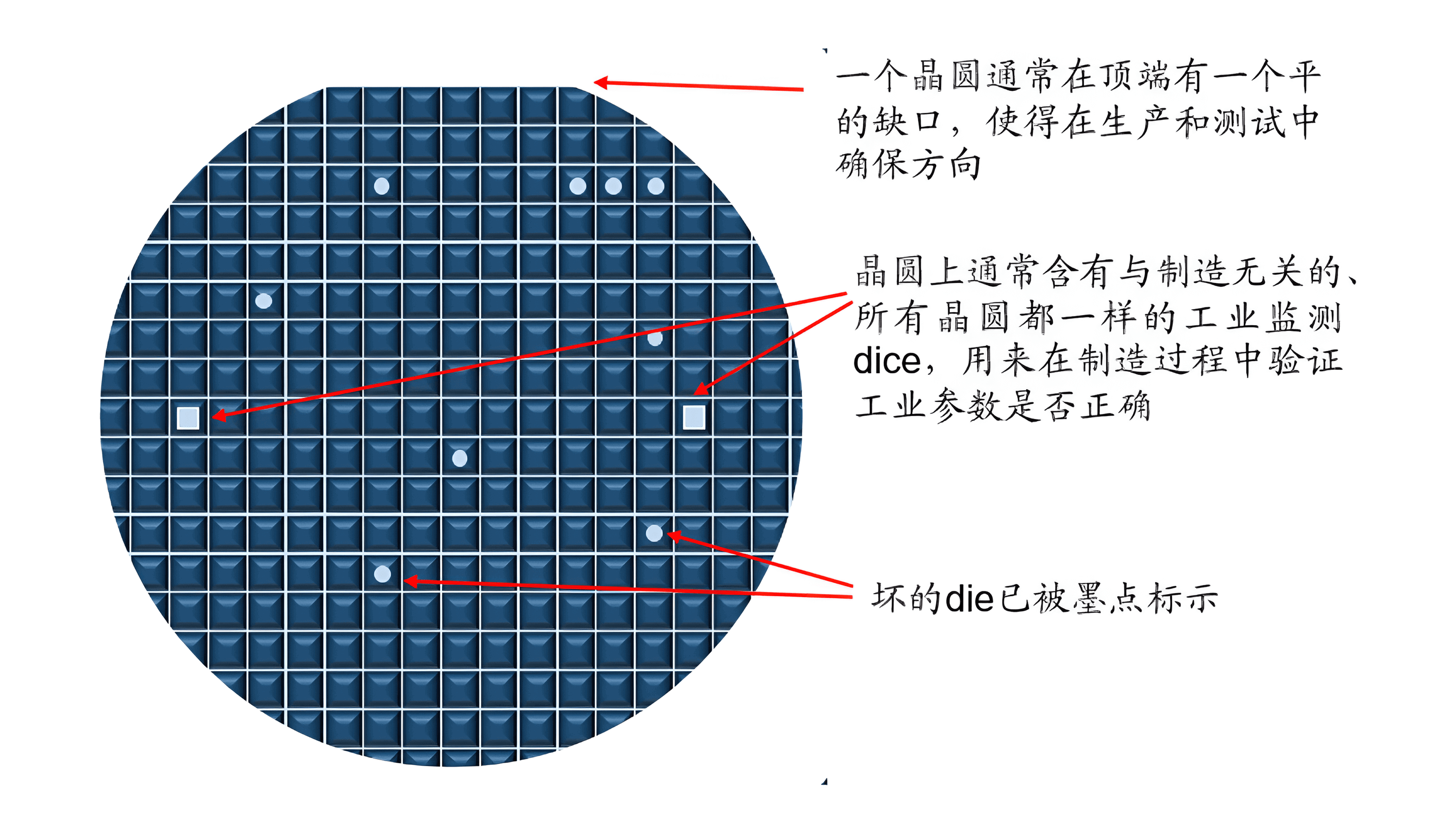
CP Test and FT Test
CP (Chip Probe) test is a performance and functional test of the chip conducted by probing the chip pins while the chip is still in the wafer stage. FT (Final Test) is the final test conducted after the chip is packaged.
Terms for Testing Equipment
- DUT (Device Under Test): The device being tested, external signals are applied to its pins for testing. Also known as UUT (Unit Under Test).
- DPS (Device Power Supplies): Devices that directly provide voltage and current to the DUT.
- PMU (Precision Measurement Unit): A precision measurement unit used to accurately measure the DC characteristics of a device.
- PPMU (Per Pin Measurement Unit): A PMU on each pin for measurement.
- DIB (Device Interface Board): A device interface board, also known as a LOAD board.
- PIB (Probe Interface Board): A probe interface board used for Wafer Probe.
- PDP (Prober docking plate): A docking plate for the probe station.
- PROBE CARD: A PCB with probes used for Wafer Probe.
- BINNING: Sorting the DUT based on test results.
- MANIPULATOR: A structure that supports the test head and allows it to move in multiple directions.
- HANDLER: Full name IC pick up and place handler, an automatic sorting machine used to place the DUT in the test head socket.
- PROBER: A probe station, a mechanical unit that moves the chip under the test probes.
Parameters in Testing
- VCC: Power supply for TTL devices.
- VDD: Power supply for CMOS devices.
- ICC: Drive current for TTL devices.
- IDD: Drive current for CMOS devices.
- VSS: Provides a return path for the power supply.
- GND: Reference level, often equivalent to VSS in single power supply devices.
- IDD: Current consumed from CMOS devices.
- ICC: Current consumed from TTL devices.
- VIH: Minimum voltage limit for high-level input (not recognized as 0).
- VIL: Maximum voltage limit for low-level input (not recognized as 1).
- VOH: Minimum voltage limit for high-level output (not recognized as 0).
- VOL: Maximum voltage limit for low-level output (not recognized as 1).
- IIH: Maximum input current allowed when the input pin is at a high logic level.
- IIL: Maximum leakage current allowed when the input pin is at a low logic level.
- IOH: Drive/pull current (source) when the output pin is at a high logic level.
- IOL: Sink current when the output pin is at a low logic level.
- IOZH: Maximum current allowed when the output pin is at a high logic level and in a high-impedance state.
- IOZL: Maximum current allowed when the output pin is at a low logic level and in a high-impedance state.
- Propagation Delay: The time interval from the signal input to the change in the output signal.
- Rise Time: The time required for a signal to rise from 10% to 90% of the high-level voltage.
- Fall Time: The opposite of the above.
Hot Switching
Hot switching, also known as current-carrying switching, refers to the switching of relays while current is flowing (there can be voltage, as long as the voltage on both sides is consistent). This may shorten the lifespan of the relay or damage it, so programming is required to avoid such situations.
Latch-up
When a pin is subjected to excessive voltage, it causes a large current to flow in CMOS devices, resulting in local circuit damage or even burnout.
Stuck-At Fault
Stuck-At Fault (SAF) refers to a signal pin that is stuck at a 0/1/Z level due to manufacturing defects, causing a fault.
Binning
Binning is the process of grouping DUTs based on test results. For example:
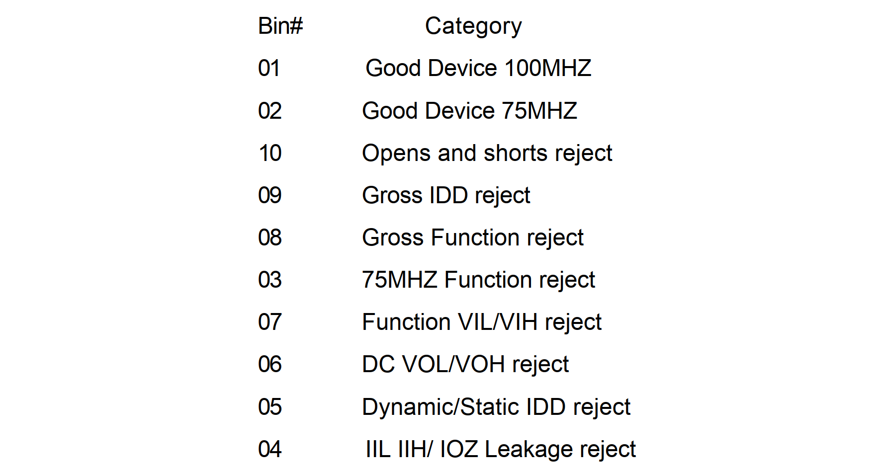
Hard Binning refers to using machines like Handlers to classify into two groups; Soft Binning refers to recording and distinguishing defective products in software without physical classification.
The binning process requires at least two bins to differentiate whether a test result passes or fails.
Program Flow
The design of the program flow is crucial for the entire testing process. For example, some DC tests require pre-processing (setting specific device logic, such as functional testing), and the lack of pre-processing will render the results of subsequent steps meaningless.
The design of the program flow needs to consider many factors, such as the test volume, which parameters need to be tested, and how to perform binning. Flowcharts are usually used to present the program flow and ensure that it meets the requirements.
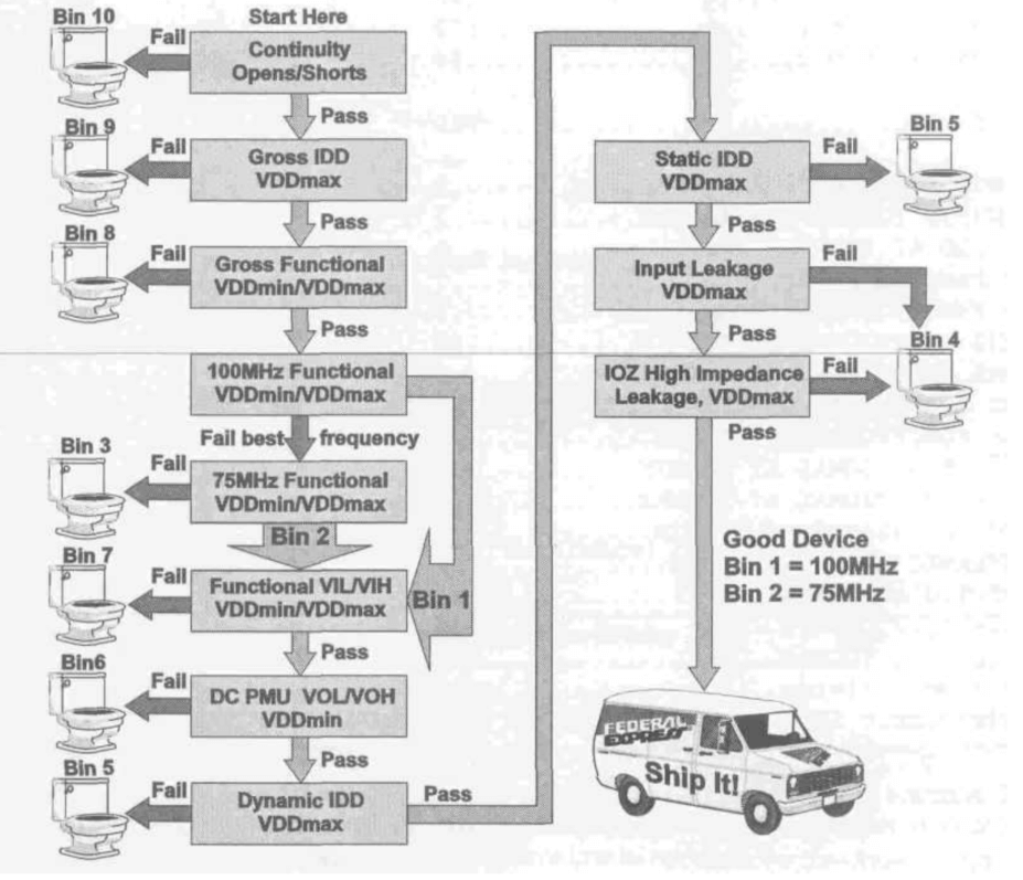
Basic test items:
- Contact/Continuity Test: This test is used to check for open or short circuits in the device pins.
- DC Parametrics Test: This test is performed to verify the DC current and voltage parameters of the device, including IDD.
- Digital Functional Test: This test is conducted to test the logical functions of the Device Under Test (DUT).
- AC Timing Test: This test is carried out to verify the AC specifications of the device, including output signal quality and signal timing parameters.
- Mixed Signal Test: This test is performed to validate the logic of both the analog and digital circuits of the DUT.
- Other test items include RF devices, automotive devices, memory devices, power management devices, RFID devices, and high-speed digital devices.
References and Acknowledgements
- "The Fundamentals Of Digital Semiconductor Testing"
- Semiconductor Testing Equipment: Integration of Core and Screen, Convergence of Light and Electricity
- In-depth Explanation of Latch-up
- https://www.eefocus.com/ansonguo/blog?p=1
Original: https://wiki-power.com/
This post is protected by CC BY-NC-SA 4.0 agreement, should be reproduced with attribution.This post is translated using ChatGPT, please feedback if any omissions.