Signal Integrity - Transmission Lines 🚧
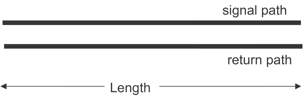
A transmission line is an ideal component consisting of two wires of specific length, referred to as the signal path and the return path (reference path). Transmission lines possess two essential characteristics: characteristic impedance and delay.
Signal Transmission Modes
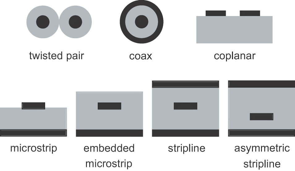
To understand signal transmission, it's crucial to consider both the signal path and the return path. How do we determine these paths? If the two wires are identical (e.g., twisted pair cables), there's no strict differentiation. However, for microstrip lines, the plane is typically designated as the return path. It's worth noting that in the realm of signal integrity, we use the concept of the "return path" instead of "ground" because the scenarios to be analyzed are far more complex than simple grounding.
Once a signal enters a transmission line, it propagates through the medium at the speed of light. We can represent the signal as the voltage difference between adjacent points on the signal path and the return path:
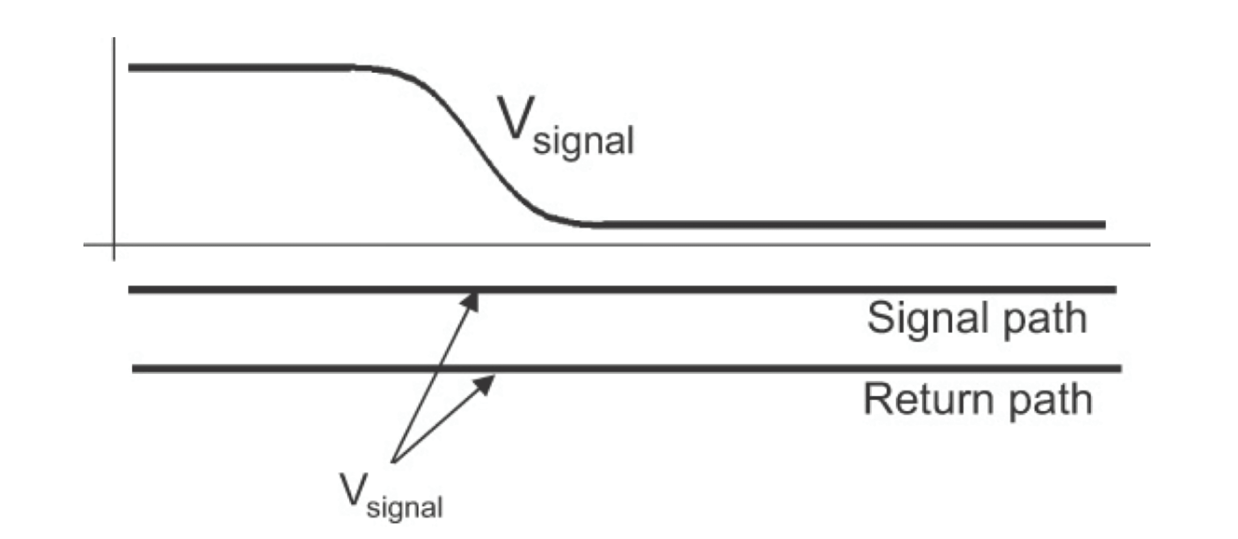
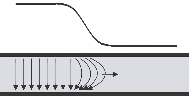
Assuming a pair of sufficiently long transmission lines with open ends, current meters connected at the source and destination, and the signal's current being detected. In practical experiments, it can be observed that as the signal first enters the signal path, current is already detected on the return path. Thus, the current loop does not flow from the source to the destination and then back through the return path but is generated by the potential difference between the signal and the return path (similar to charging a capacitor). As the signal propagates, the location where current is generated continuously shifts forward.
Uniform Transmission Lines and Balanced Transmission Lines
When classifying transmission lines, they can be categorized based on two characteristics: the uniformity of their cross-section along the length and the similarity and symmetry of the two conductors.
If the cross-section is the same at any position along the conductors, it's called a uniform transmission line or controlled impedance transmission line, examples of which include twisted pair cables and microstrip lines with strip conductors:
One of the objectives of signal integrity design is to design all high-speed interconnects as uniform transmission lines and minimize the length of non-uniform transmission lines.
The other classification criterion is the similarity or symmetry of the two conductors. If both conductors have identical shapes and sizes, it's termed a balanced transmission line, such as twisted pair cables. An example of an unbalanced transmission line is coaxial cable because its center conductor has a smaller cross-sectional area than the outer layer.
Signal Propagation Velocity
The velocity of signal propagation on a transmission line is not dependent on the speed of electrons within the conductor.
If you know the number of electrons passing through the cross-sectional area of the conductor per second, the electron density within the conductor, and the cross-sectional area of the conductor, you can calculate the speed of the electrons within the conductor. This is because the current in the conductor (\(I\)) can be calculated using the following formula:
Here, \(\Delta Q\) represents the electric charge passing through the conductor in \(\Delta t\) time (in coulombs), \(q\) is the charge carried by a single free electron (a constant of \(1.6\times 10^{-19}\) coulombs), \(n\) is the electron density (in \(\#/m^3\)), and \(A\) is the cross-sectional area of the conductor (in square meters). Therefore, you can calculate the electron velocity (in meters per second) as:
In common dielectrics, the speed of electron motion is quite low. For example, in a copper conductor with a diameter of 1mm (with copper atoms spaced about 1nm apart, and each copper atom providing two free electrons, resulting in an electron density of approximately \(10^{27}/m^3\)), the velocity of electrons with a current of 1A is approximately 1cm/s. This demonstrates that the speed of electrons is far lower than the speed of signal propagation.
Furthermore, reducing the resistance of interconnections does not necessarily increase the speed of signal propagation. Only in extremely rare circumstances does the resistance of interconnection lines slightly affect signal propagation speed. In general, low conductor resistance does not imply fast signal transmission.
The principle of signal transmission through electrons relies on the interaction between the electrons.
You can imagine a conductor as a long tube filled with marbles. If you push one marble at one end, another marble will be squeezed out almost simultaneously at the other end. In this case, the speed at which the marbles carry the signal is much faster than the actual speed of the marbles' motion. Similarly, when electrons in a conductor are pushed by neighboring electrons, the speed of signal propagation does not depend on the individual electron's speed but is influenced by the interplay between the electrons.
As the signal is transmitted, it creates an alternating electromagnetic field in the conductor and the surrounding space between the signal and the return path. The factor determining the speed of signal propagation is the establishment and propagation speed of this electromagnetic field.
The speed of electromagnetic field variation (field chaining) can be calculated by the following formula:
Where:
- \(\varepsilon_0\) represents the permittivity of free space, with a value of \(8.89\times 10^{-12}F/m\).
- \(\varepsilon_r\) represents the relative permittivity of the material, which is 1 in air.
- \(\mu_0\) stands for the permeability of free space, with a value of \(4\pi\times10^{-7}H/m\).
- \(\mu_r\) represents the relative permeability of the material, which is nearly 1 for most interconnect materials. Substituting the constants yields:
Compared to air, the relative permittivity \(\varepsilon_r\) of other materials is always greater than 1, and the speed of light is approximately \(12 inch/ns\). This means that the actual speed of signal in the interconnect is less than \(12 inch/ns\), and it can be calculated as:
Relative permittivity is often simply called permittivity. The value of permittivity for most polymers is around 4. In general, permittivity decreases with increasing frequency, but in common PCB materials, this change is relatively small. For example, the permittivity of FR4 varies between 3.5 and 4.5, while high-speed materials fluctuate between 3 and 4. Based on the formula, it can be inferred that the signal velocity in FR4 is approximately \(6 inch/ns\) (not considering the electromagnetic field effect of air as the medium).
Advance of Spatial Extension
The rising edge RT of a signal usually represents the time it takes for the signal to change from 10% to 90% of the maximum voltage. As the signal propagates on transmission lines, it pushes this edge forward, creating spatial extension:
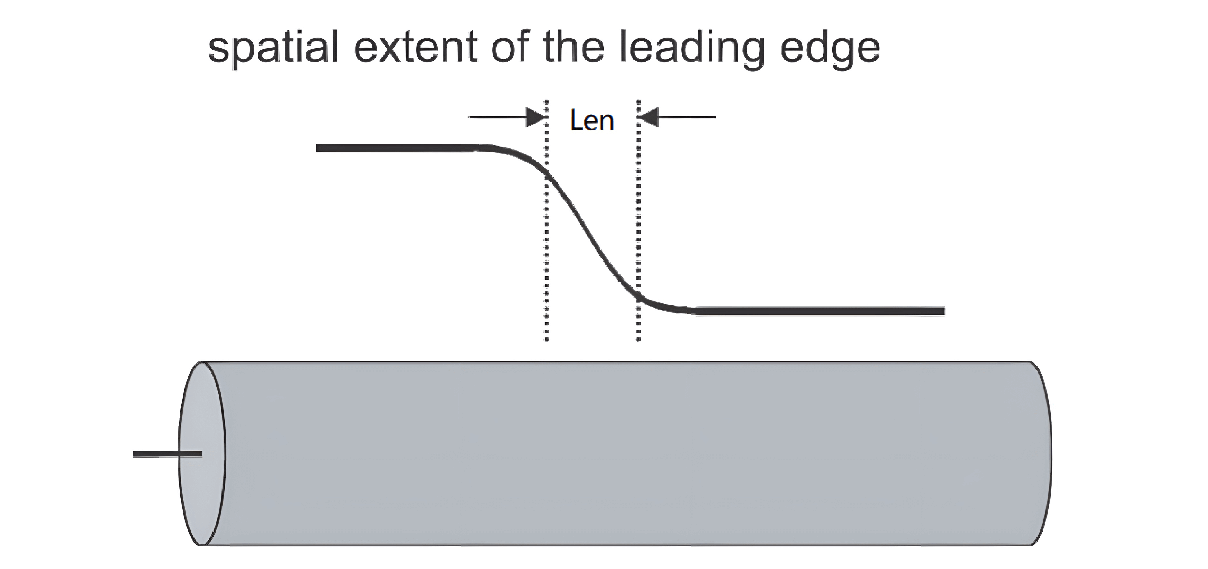
The length of this extension depends on the signal velocity and the rising edge time:
Assuming a signal velocity of \(6 inch/ns\) and a rising edge duration of \(1 ns\), the spatial extension of the rising edge is $6 inches". The signal pushes forward along this 6-inch-long edge.
Distributed Capacitance of Transmission Lines
When multiple conductors are present, capacitance exists between each pair of conductors. For traces on a PCB, due to the long spatial structure, each part of the trace has capacitance with the surrounding conductors, distributed across the entire length of the trace. Therefore, the capacitance of a transmission line is distributed. As the signal moves forward, it can feel the presence of capacitance at each step.
In high-speed interconnect models, many phenomena such as impedance mismatches, reflections, crosstalk, etc., are related to the distributed capacitance between conductors.
Unit Length Capacitance
For PCB transmission lines with constant cross-sectional area, the capacitance can be represented using a lumped capacitance model, where the capacitance parameters are represented per unit length. This way, the total capacitance is proportional to the length of the transmission line, making it convenient for modeling.
Lumped elements: Refers to elements whose size is much smaller than the electromagnetic wave wavelength relative to the circuit's operating frequency. For a signal, the element's characteristics remain fixed at all times, regardless of the frequency.
The premise of using unit length capacitance to represent the capacitance effect of a transmission line is that there is no electric field component along the direction of the transmission line, i.e., the propagation of electromagnetic waves approximates a uniform plane wave. PCB traces satisfy this condition.
Distributed Inductance of Transmission Lines
Impedance mismatches, reflections, crosstalk, ground bounce noise, etc., are also related to distributed inductance. Each part of the trace on the PCB has self-inductance and mutual inductance with surrounding conductors. Inductance is distributed across the entire length of the trace, and the signal can feel the presence of inductance at each step.
Loop Inductance
Because transmission lines can treat signals and return paths as a unified entity, signal current and return current coexist and form a complete current loop, making it more convenient to use loop inductance analysis. The calculation formula for loop inductance is:
Where \(L_{SS}\) represents the self-inductance of the signal path, \(L_{FS}\) represents the self-inductance of the return path, and \(L_{SFm}\) represents the mutual inductance between the signal and return paths.
By considering the loop as a whole, loop inductance describes the inductance characteristics of the loop itself, equivalent to the self-inductance of the loop itself.
Unit Length Inductance
For modeling convenience, the inductance of a transmission line can also be equivalently represented as a series of multiple inductances in parallel. Dividing the transmission line into many small segments of unit inductance (each segment includes the signal and return paths), with a length of \(\Delta Z\), the larger \(\Delta Z\), the larger the area formed by the signal and return paths, and consequently, the larger the magnetic flux. Since the magnetic flux is linearly related to the area of \(\Delta Z\), it is also linearly related to \(\Delta Z\). Therefore, as long as the unit length of loop inductance is known, the loop inductance for any length can be determined.
Transient Impedance and Characteristic Impedance √
Based on the previous definition, we know that impedance refers to the ratio of voltage to current at a specific position on the transmission line. Since the transmission line is not necessarily uniform, the impedance encountered by the signal at each step may be different. This is referred to as transient impedance.
If the transmission line is uniform, then a single impedance value can represent the impedance characteristics of the entire transmission line. This impedance value is known as the transmission line's characteristic impedance and can be represented using unit length inductance and unit length capacitance:
The commonly used 50Ω impedance in PCB design refers to characteristic impedance. For FR4 substrate material, when the line width is twice the substrate thickness, the characteristic impedance of microstrip lines is 50Ω. When the spacing between transmission lines is the same, a higher characteristic impedance leads to more serious crosstalk issues, while a lower characteristic impedance results in greater power loss. Thus, 50Ω is a relatively balanced value and has become a standard. However, it does not mean that all interconnections must be 50Ω; impedance can still be customized according to requirements.
Factors Affecting Characteristic Impedance √
There are four main factors that affect characteristic impedance: line width, dielectric thickness, dielectric constant, and copper foil thickness.
Line width affects unit length inductance and capacitance, thus affecting characteristic impedance. For inductance, a wider line width results in lower inductance, as the current is more dispersed. Conversely, a narrower line width concentrates the current, increasing inductance. For capacitance, a wider line width concentrates more of the electric field lines between the trace and the plane in the dielectric region, leading to higher unit length capacitance (analogous to a parallel-plate capacitor where greater area results in greater capacitance); a narrower line width results in lower capacitance. In summary, wider line widths lead to lower characteristic impedance.
Increasing dielectric thickness widens the gap between two conductors, reducing mutual inductance, and consequently increasing unit length inductance, leading to an increase in characteristic impedance.
The dielectric constant affects characteristic impedance by influencing unit length capacitance. As the dielectric constant increases, capacitance also increases, resulting in a lower characteristic impedance.
Greater copper foil thickness reduces inductance and increases capacitance, resulting in a lower impedance.
Transmission Line Driving and Internal Resistance
The driver can be equivalently represented as a voltage source with high-speed switching plus internal resistance:
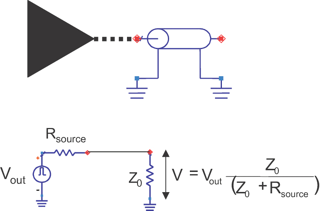
When open-circuited, the voltage applied to the transmission line is very close to the source voltage. The magnitude of the internal resistance depends on the device's manufacturing process, typically ranging from 5-60Ω. When connected in series with the internal resistance in the circuit, it can be considered as a voltage divider, generating a voltage drop.
To better drive the transmission line, the driver's internal resistance should be as small as possible compared to the characteristic impedance of the transmission line. For example, if the characteristic impedance of the transmission line is 50Ω, the internal resistance should be less than 10Ω. If the driver's internal resistance is very low, it is known as a line driver, capable of delivering most of the voltage to the transmission line.
To calculate the driver's internal resistance, the transmission line does not need to be connected. The driver is directly connected to external resistors, and the voltage across the large and small resistors is measured separately. With this information, the internal resistance can be calculated using the equation.
Return Path and Reference Plane
Current always flows in a loop, and where there's a path, there's a return path.
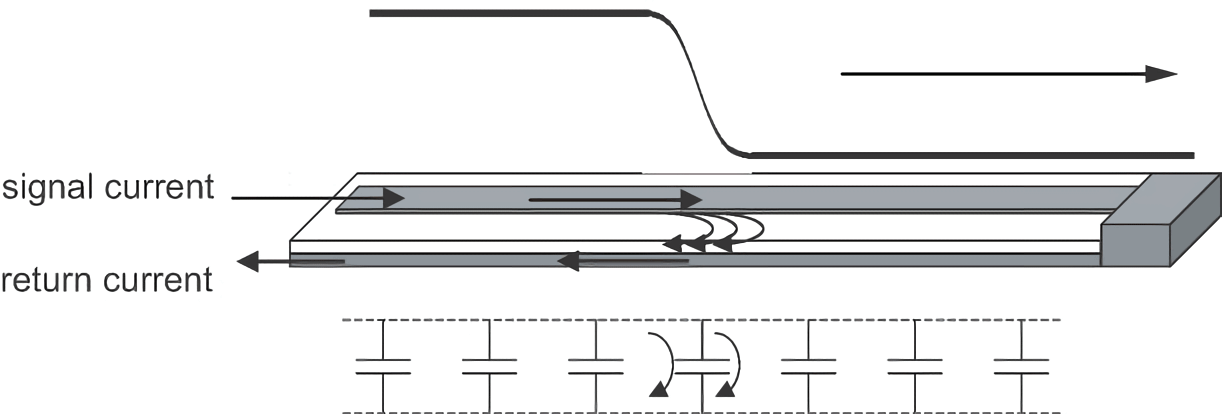
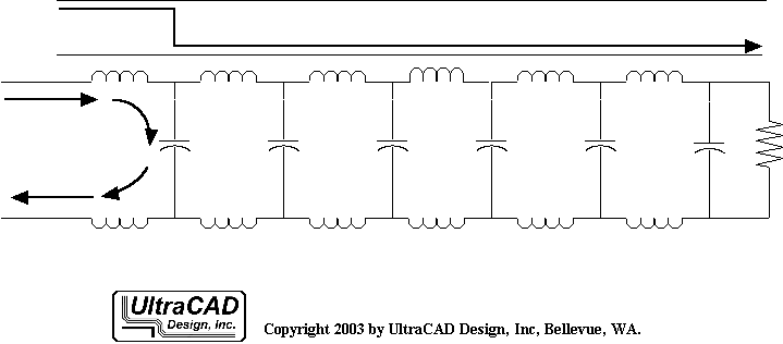
According to the zero-order model of the transmission line, a series of small capacitances exist between the transmission line's signal and the return path. Voltage, like a wave, changes as it passes the edge of these areas, causing current to flow through the capacitance to the return path.
Once a signal enters the transmission line, it propagates outward in the form of waves. Current flows in the loop formed by the signal path, line capacitance, and the return path. The leading edge of this current loop and the leading edge of the voltage propagate outward simultaneously. Therefore, the transient impedance experienced by the signal is the ratio of signal voltage to current.
If the return path is a plane (different from the signal trace), it is referred to as the reference plane. For surface signal traces, they can only form transmission lines with the adjacent inner plane, meaning they have only one reference plane. However, for inner layer traces, there are two adjacent planes above and below, so there are two reference planes. Planes located in different layers and overlapping with the signal traces can serve as reference planes, forming transmission lines.
The return current on the reference plane is not evenly distributed across the entire reference plane; it exhibits a skin effect and concentrates near the area directly below the trace. The magnitude of the return current on the reference plane of a surface microstrip line is equal to the signal current. For stripline traces, because there are two reference planes (above and below), the return current concentrates near the upper and lower sides of the signal line, distributed proportionally based on the distance to the planes. As the signal frequency increases, the current gets pushed closer.
Transmission Line Delay 🚧
Signals take some time to travel from the source end to the destination end, resulting in a certain delay.
First-Order Model of an Ideal Transmission Line 🚧
An ideal transmission line possesses two critical features: a constant characteristic impedance and a corresponding delay. In the first-order model, based on the zero-order model, each small section of the signal and return path conductors is abstracted as a loop inductance:
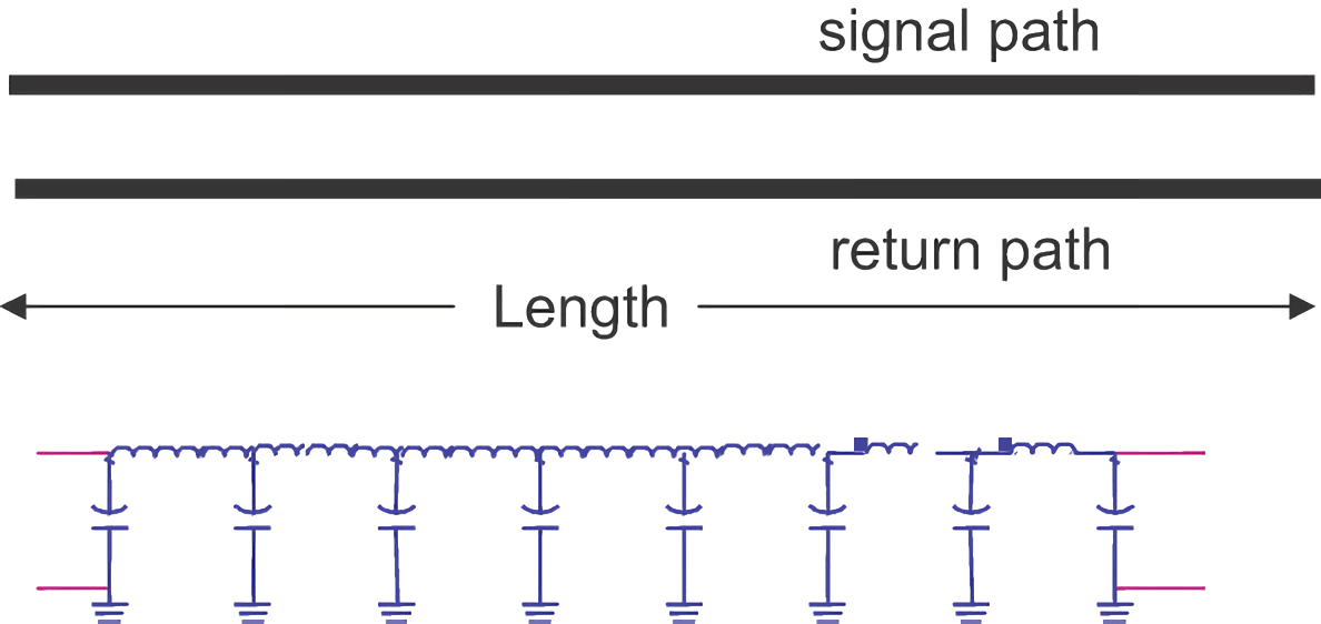
When the capacitance and inductance are infinitesimal, and the number of LC circuit sections tends to infinity, the unit-length capacitance \(C_L\) and unit-length inductance \(L_L\) become constants, which are the line parameters of the transmission line. If the total length of the transmission line is \(Len\), then the total capacitance and inductance are:
As a result, the characteristic impedance \(Z_0\) and delay \(T_D\) of the transmission line are as follows:
Because the characteristic impedance and delay of the transmission line must be consistent with the results of the zero-order model, some equations can be derived.
Since the signal velocity depends on the material's dielectric constant \(\varepsilon_r\) (epsilon), which in turn depends on the unit-length capacitance and inductance, we obtain the equation:
References and Acknowledgments
- "Signal Integrity and Power Integrity Analysis"
- "Signal Integrity Unveiled - Dr. Yu's SI Design Notes"
Original: https://wiki-power.com/ This post is protected by CC BY-NC-SA 4.0 agreement, should be reproduced with attribution.
This post is translated using ChatGPT, please feedback if any omissions.