ADC - Static Parameters
This post was originally written in English.
Analog to Digital Converter (ADC) is a device to converts analog signals into a sequence of digital data.
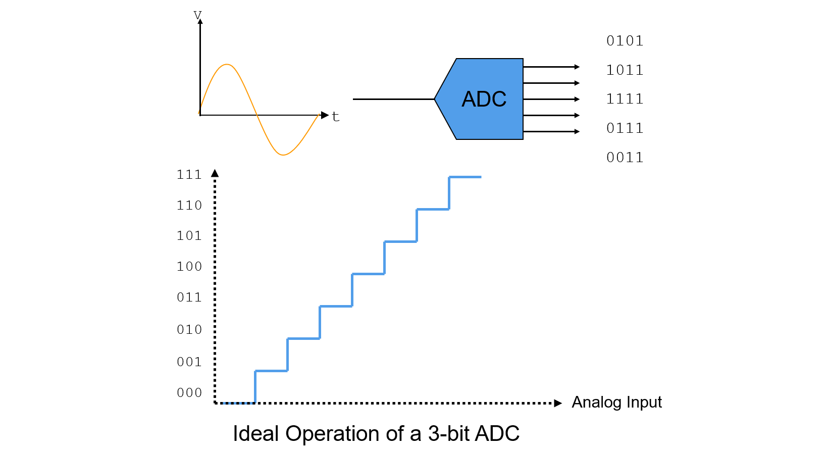
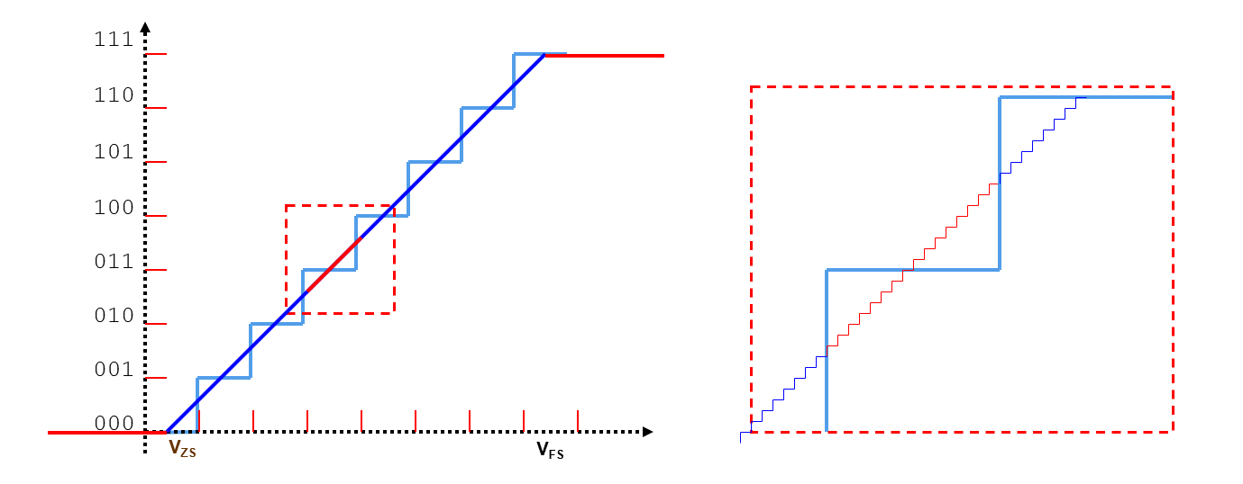
Though ADC's ideal transfer function should be a straight line, but actually is a uniform staircase, that the number of steps corresponds to the number of digital output codes. Since analog is continuous and digital is discrete, quantization error will be introduced in the procedure.
Static Parameters
ADC's static parameters mainly contain:
- LSB Size
- Full Scale Range (FSR)
- Offset Error
- Gain Error
- Differential Non-Linearity Error (DNE or DNL)
- Integral Non-Linearity Error (INE or INL)
LSB Size
The width of one step is defined as 1 Least Significant Bit (LSB). The resolution of an ADC is normally expressed as number of bits (digital output code). An ADC with an n-bit resolution has \(2^n\) possible digital codes (\(2^n\) step levels).
For an ideal ADC, LSB represents all of the each code's width.
Full Scale Range (FSR)
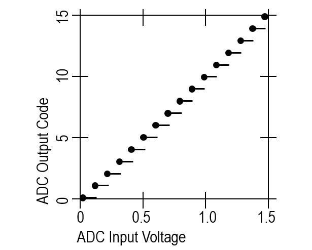
For example, for a 3 bit converter, there are:
- 8 horizontal steps
- 7 transitions
- 6 steps between 7 transitions
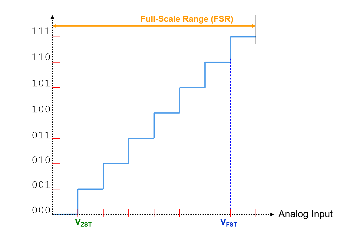
- Zero Scale Range Transition Voltage (\(V_{ZST}\)): Voltage of the analog input signal when the first transition is recorded.
- Full Scale Range Transition Voltage (\(V_{FST}\)): Voltage of the analog input signal when the last transition is recorded.
- Full Scale Range (FSR): Maximum extreme of the analog input signal supplied to the ADC. \(FSR = (V_{FST}-V_{ZST}) + 2 LSB\), \(V_{FSR(refer to VZS)} = (V_{FST}-0.5LSB)-(V_{ZST}-0.5LSB) + 2 LSB\)
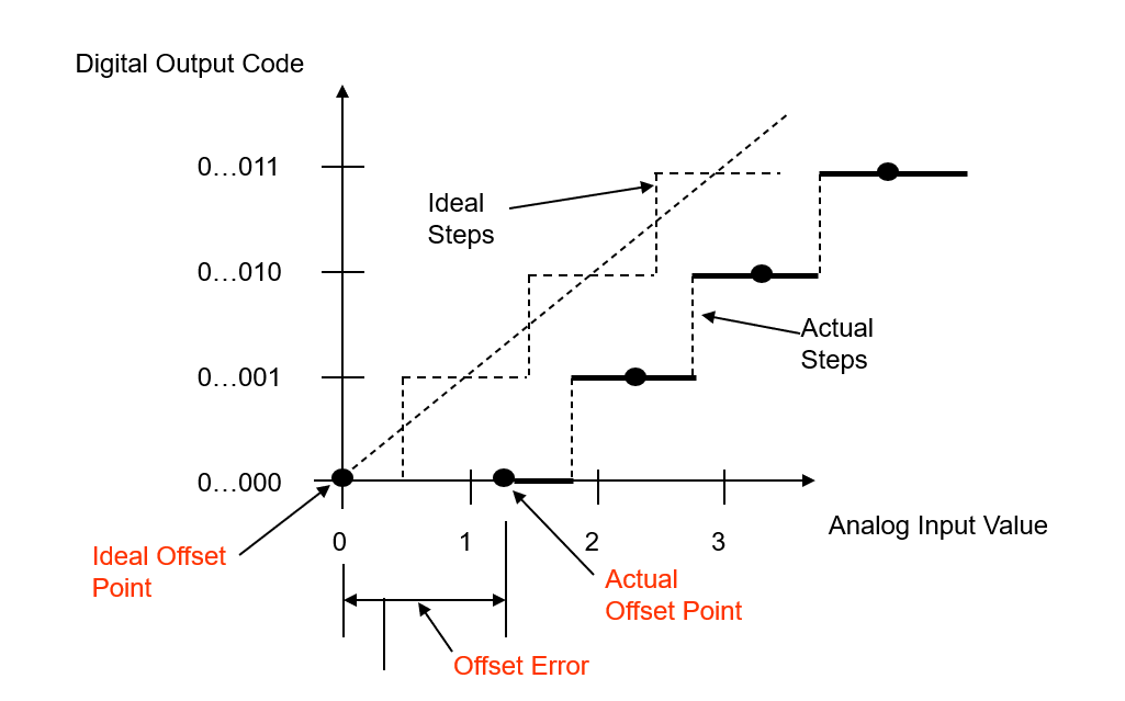
Offset Error
Offset Error (Zero-Scale Error) is the difference between ideal and actual offset (initial) points. It is measured from the midpoint of the zero step (ideal to actual) for the ADC.
Where
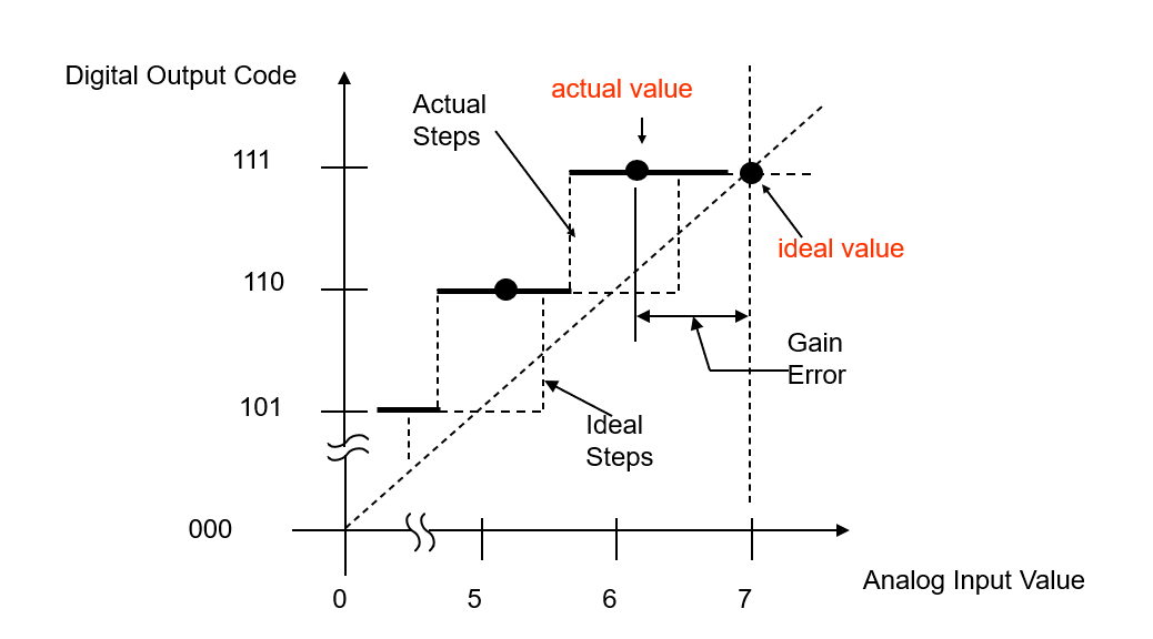
Gain Error
Gain Error is the difference between ideal and actual gain points on the transfer function (after the offset error has been corrected to zero). It is measured from the midpoint of the full step for the ADC.
Where
Differential Non-Linearity Error (DNL)
Differential Non-Linearity Error (DNL) is the difference between an actual step width and an ideal step width (1 LSB). It's a measure of "small-signal" linearity error, and is measured from the difference in the analog input voltage between 2 adjacent transitions and the device's average LSB.
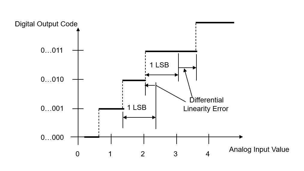
Equations to describe DNL:
another image to decribe DNL:
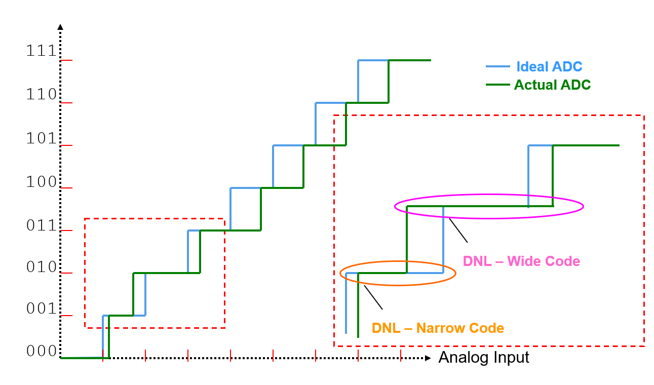
If DNL exceeds is too large, one or more codes will be missing and never receive an output.
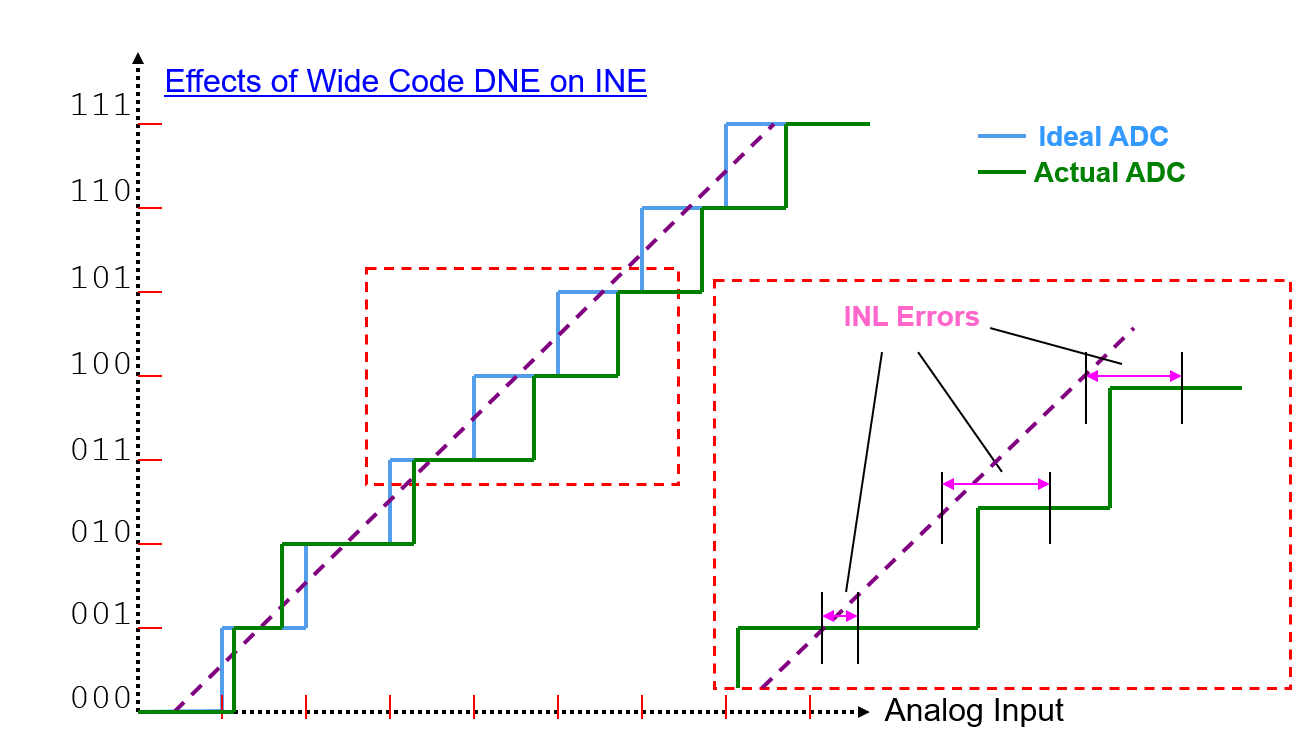
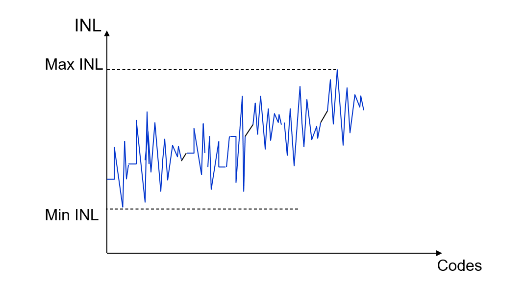
Integral Non-Linearity Error (INL)
Integral Non-Linearity Error (INL) is the cumulative effect at any given input of all differential non-linearity values. It is a measure of "large-signal" linearity error. INL at any point along the curve is the deviation of the ideal linearity line.
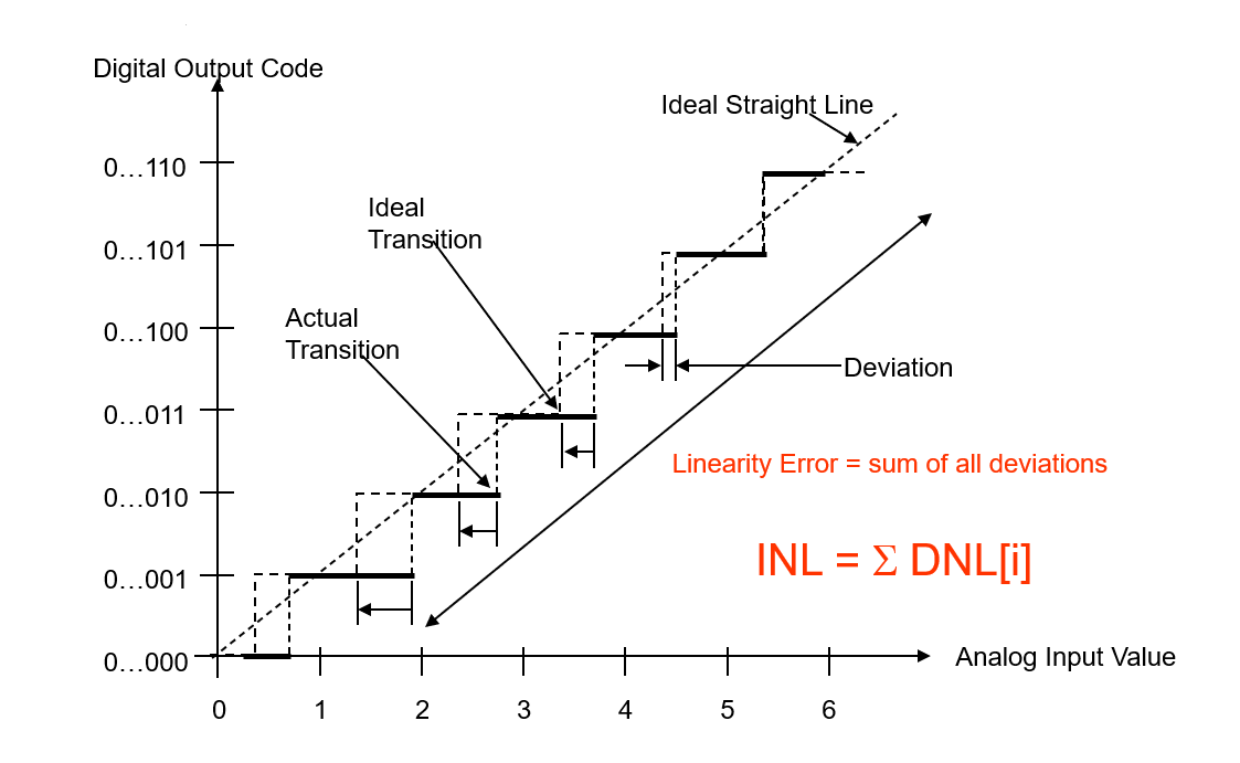
The deviations are measured at the transition points from one step to the next for the ADC. INL is the deviation of the values of the actual step function to the ideal straight line function.
Equations to describe INL:
How to Test Static Parameters
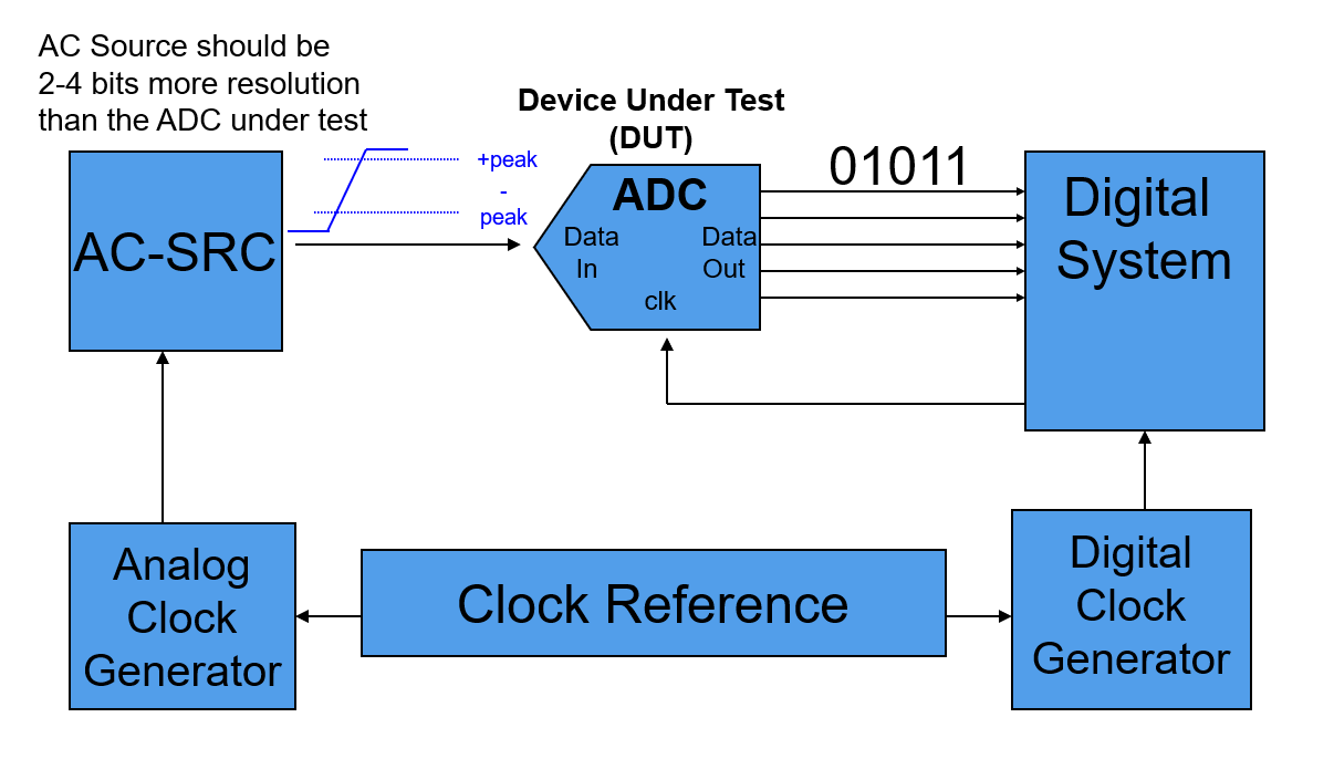
Test System Setup
Test system setup for ADC static parameter tests:
Since the ADC voltage-to-code transfer curve is a many-to-one mapping function:
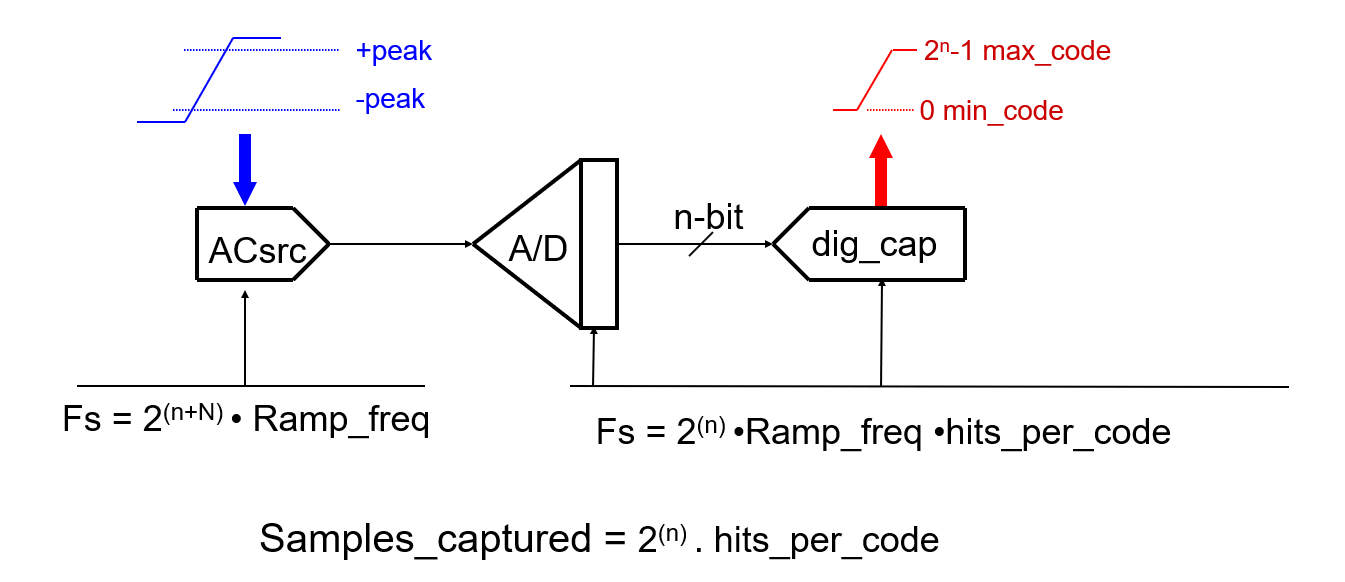
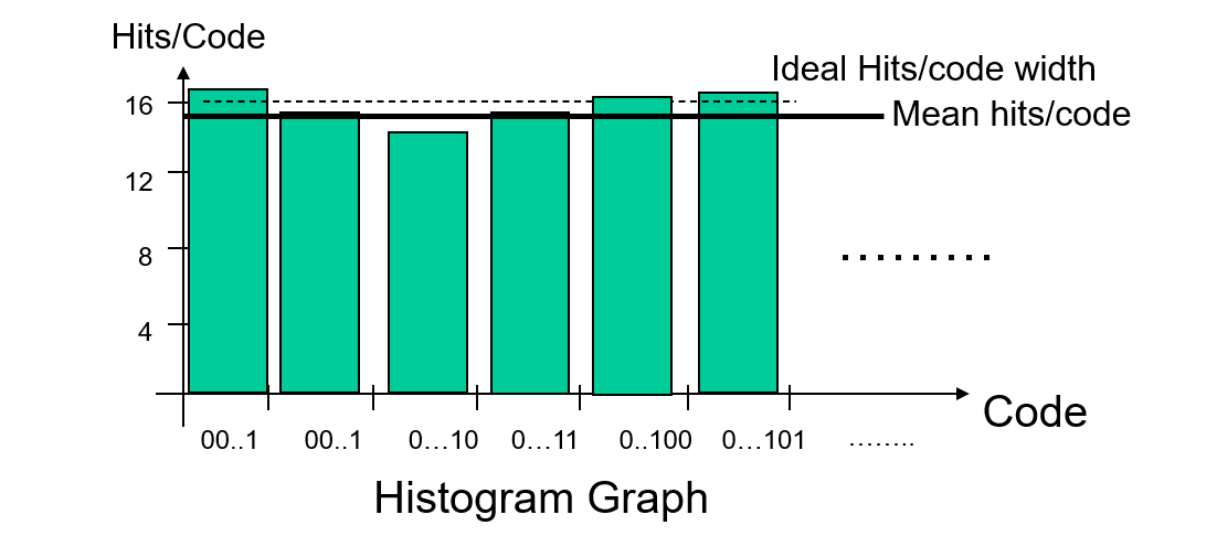
We use linear ramp histogram method (code width measurement) practically. The input ramp is slow enough to give a statistically relevant "number of hits per code".
Block diagram of signal setup:
Tests Concept
Procedure of testing the static parameters of an ADC DUT is listed below.
1. Make a ramp wave segment for AC SRC
The input ramps goes above and below ±Fs to assure that all codes are covered:
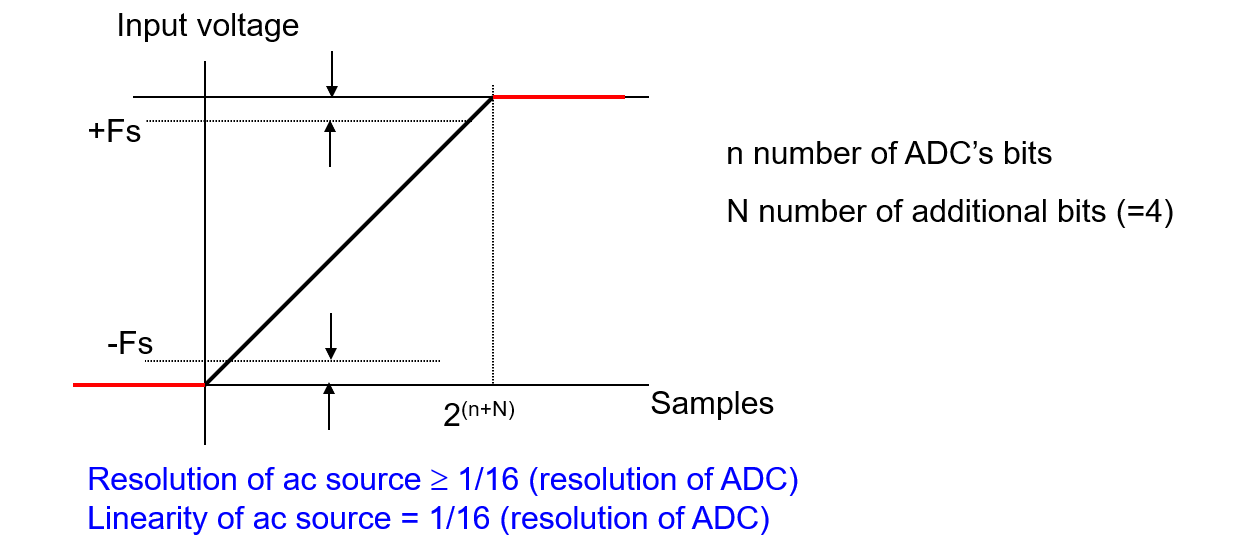
2. Take data between the start (min+1, e.g. 0…01) and the end (max-1, e.g. 1…10) of the ramp. That gives \(2^n – 2\) codes' worth of data
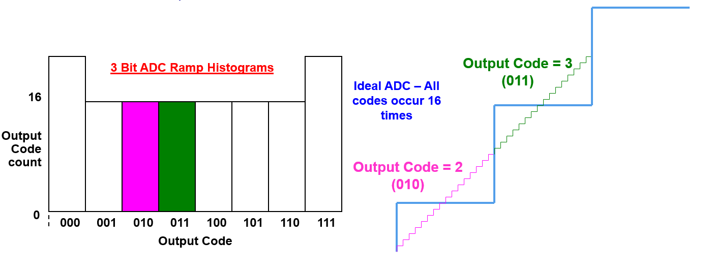
Voltage applied must be wider than the full-scale range to cover all transitions. 16 steps in-between each code transition is shown below:
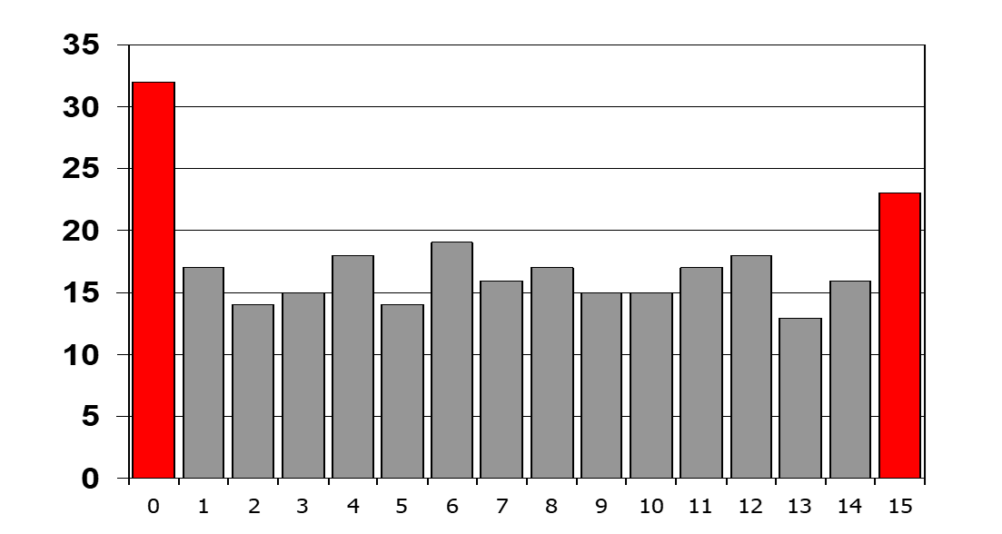
for the ideal ADC DUT, 16 output codes are appear in the same times:
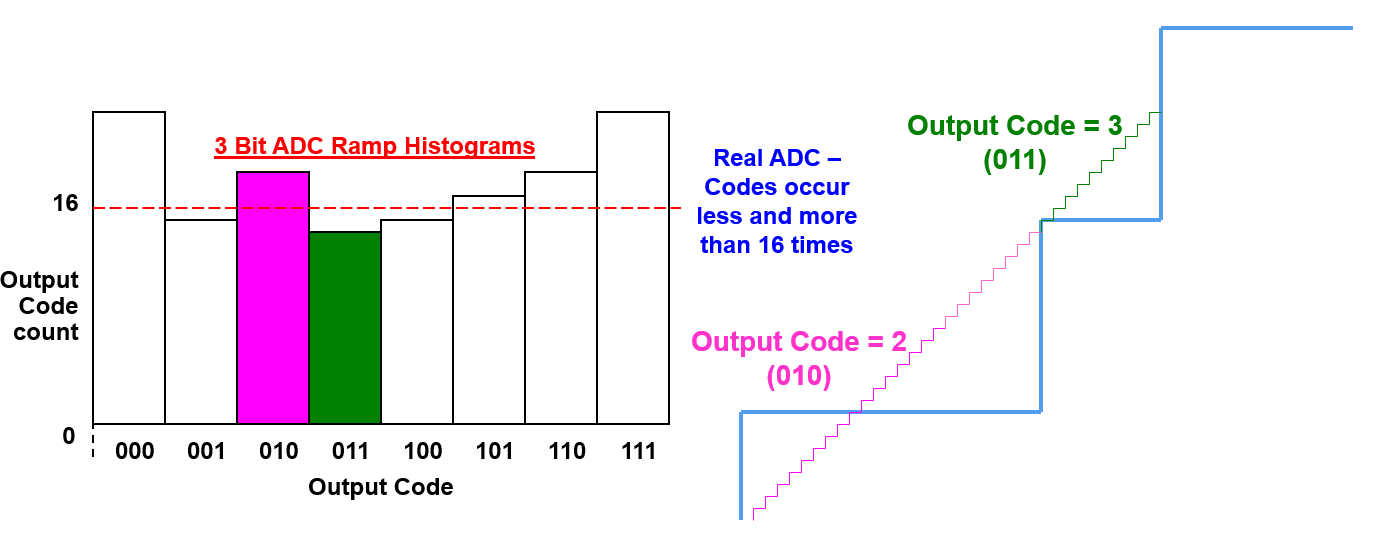
However, a real device will have a count more than 16 times for wider codes, and less than 16 times for narrower ones (But sum of the total occurrence should be still \(2^{bits}\) times of 16):
3. Calculate for DNL for each step
Where \(Hits[i]\) represents the Actual Output Code Count, and \(\frac{\sum Hits[i]}{2^n-2}\) represents the Ideal Output Code Count.
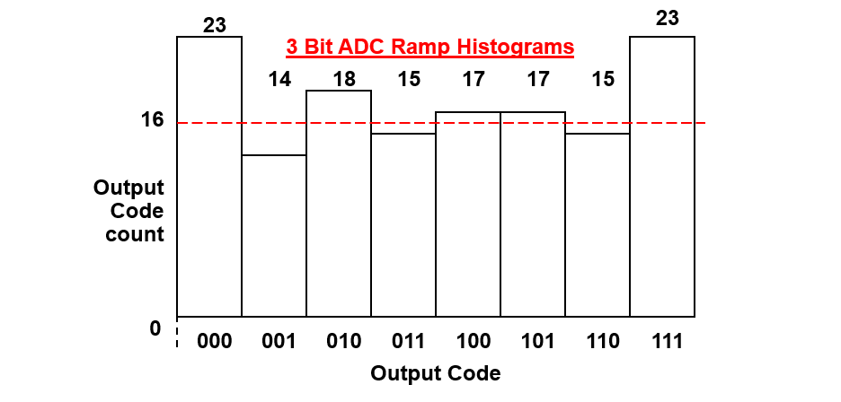
For an example historam graph as shown below:
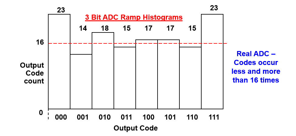
for \(DNL[1](Code 001)\),
- Actual Output Code Count = 14
- Idea Output Code Count = (14 +18 +15 + 17+ 17 + 15) / (8 -2 ) = 16.
Therefore \(DNL[1] (Code 001) = (14-16)/16 \ LSB => -0.125 \ LSB\).
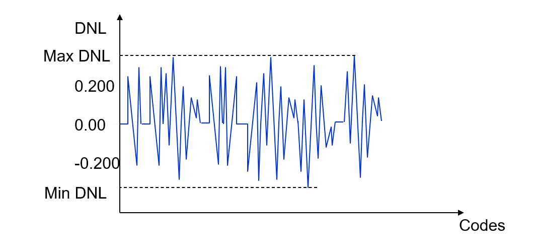
4. Get the max and min DNL
5. Calculate for INL for each step
INL is the cumulative value of the first DNL to the DNL[i] (except zero and full scale DNL):
Note that \(DNL[0]\) is not used,
For an example graph below,
6. Get the max and min INL
References & Acknowledgements
- Fundamentals of Testing Using ATE
- The-Fundamentals-of-Mixed-Signal-Testing_Brian-Lowe
Original: https://wiki-power.com/
This post is protected by CC BY-NC-SA 4.0 agreement, should be reproduced with attribution.